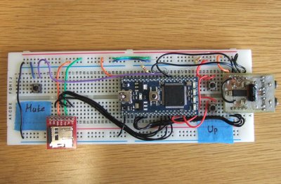
HQ Audio
The idea is to build a high quality audio module together with libraries and example projects, using the external DAC (TLV320AIC23B - http://focus.ti.com/docs/prod/folders/print/tlv320aic23b.html) from Texas Instruments. The chip is designed for audio applications with an internal 30mW per channel headphone amplifier (driving 32Ohm speakers).
Here are the DACs features borrowed from the datasheet:
- High-Performance Stereo Codec
- 90-dB SNR Multibit Sigma-Delta ADC (A-weighted at 48 kHz)
- 100-dB SNR Multibit Sigma-Delta DAC (A-weighted at 48 kHz)
- 1.42 V – 3.6 V Core Digital Supply: Compatible With TI C54x DSP Core Voltages
- 2.7 V – 3.6 V Buffer and Analog Supply: Compatible Both TI C54x DSP Buffer Voltages
- 8-kHz – 96-kHz Sampling-Frequency Support
- Software Control Via TI McBSP-Compatible Multiprotocol Serial Port
- 2-wire-Compatible and SPI-Compatible Serial-Port Protocols
- Glueless Interface to TI McBSPs
- Audio-Data Input/Output Via TI McBSP-Compatible Programmable Audio Interface
- I2S-Compatible Interface Requiring Only One McBSP for both ADC and DAC
- Standard I2S, MSB, or LSB Justified-Data Transfers
- 16/20/24/32-Bit Word Lengths MicroStar Junior is a trademark of Texas Instruments.1−2
- Audio Master/Slave Timing Capability Optimized for TI DSPs (250/272 fs ), USB mode
- Industry-Standard Master/Slave Support Provided Also (256/384 fs ), Normal mode
- Glueless Interface to TI McBSPs
- Integrated Total Electret-Microphone Biasing and Buffering Solution
- Low-Noise MICBIAS pin at 3/4 AVDD for Biasing of Electret Capsules
- Integrated Buffer Amplifier With Tunable Fixed Gain of 1 to 5
- Additional Control-Register Selectable Buffer Gain of 0 dB or 20 dB
- Stereo-Line Inputs
- Integrated Programmable Gain Amplifier
- Analog Bypass Path of Codec
- ADC Multiplexed Input for Stereo-Line Inputs and Microphone
- Stereo-Line Outputs
- Analog Stereo Mixer for DAC and Analog Bypass Path
- Volume Control With Mute on Input and Output
- Highly Efficient Linear Headphone Amplifier
- 30 mW into 32 Ω From a 3.3-V Analog Supply Voltage
- Flexible Power Management Under Total Software Control
- 23-mW Power Consumption During Playback Mode
- Standby Power Consumption <150 µW
- Power-Down Power Consumption <15 µW
- Industry’s Smallest Package: 32-Pin TI Proprietary MicroStar Junior
- 25 mm2 Total Board Area
- 28-Pin TSSOP Also Is Available (62 mm2 Total Board Area)
- Ideally Suitable for Portable Solid-State Audio Players and Recorders
We are going to use the SOIC package for our experiments (the DAC is also available in QFN and BGA packages), mainly because is it a solder friendly package and the exposed pins will help us at the debugging process (easier to probe the exposed pins compared to no leaded packages like the QFNs).
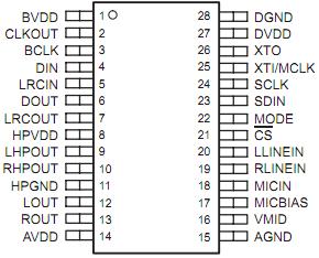
The chip uses two communication protocols. The I2S protocol (http://www.nxp.com/acrobat_download2/various/I2SBUS.pdf) for the audio data and the I2C for control of the internal DAC registers (the alternative is the SPI but we don’t have feedback after every command so it is not the preferred way).
Now it is time to move from the datasheets and the free schematic drawings to something more professional. The design of the schematic and PCB with an appropriate editor. I know that one of the preferred choices here is the Eagle and I know that we have already published a few projects and libraries using this tool. But it was time to try and something new! The Design Spark PCB from RS (http://www.designspark.com/).
It takes only a few hours to get used to this program even if you don’t have lot of experience with acronyms and tool chain processes of PCB creation and PCB software’s in general. It is simple but without the loss of the functionality needed to build professionally circuits. Of course you can import really easily your already made libraries and projects from Eagle (link). But if you want to create a new library then you should defiantly try the footprint wizard! It works perfect and it is one of my favourites out there!
So, after the library creations (audio in/out sockets and DAC) and the connection of a few lines the schematic is ready. It looks simple and it is! Just the DAC together with his basic peripheral components (100nF ceramic capacitors) and an external clock source.
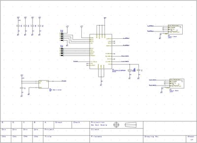
After the design of the schematic it was time to move to the PCB. From the menu bar of the Design Spark we select “Tools” and then “Translate to PCB”. The software will automatically load the layout editor with all of our components and the associated connections between those (the net-list in other words).
And the final result looks like this:
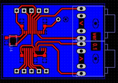
For the first experiments we’ve used the etch method. For those of you that haven’t try this method of PCB fabrication then it is time to try it. It is simple and creates good results. The only drawback is that you have to deal with chemicals and precise timings (depending on how concentrate are your fluids). After a few tries and errors you will have results defiantly better that the next one!
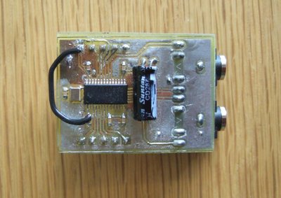
I will blame the aggressive chemicals for this one and possibly the old photo resist board! As the board is only one layer, we solder the audio in and out sockets upside down and then we wire everything for our first test board...
