Dual CANbus monitor and instrumentation cluster. Presently tuned for the Nissan Leaf EV.
Dependencies: SPI_TFTx2_ILI9341 TFT_fonts TOUCH_TFTx2_ILI9341 mbed
Fork of CANary_corrupt by
After adding the LPC1768 platform, import as a program and do not select the "update to latest revision" box
User Guide
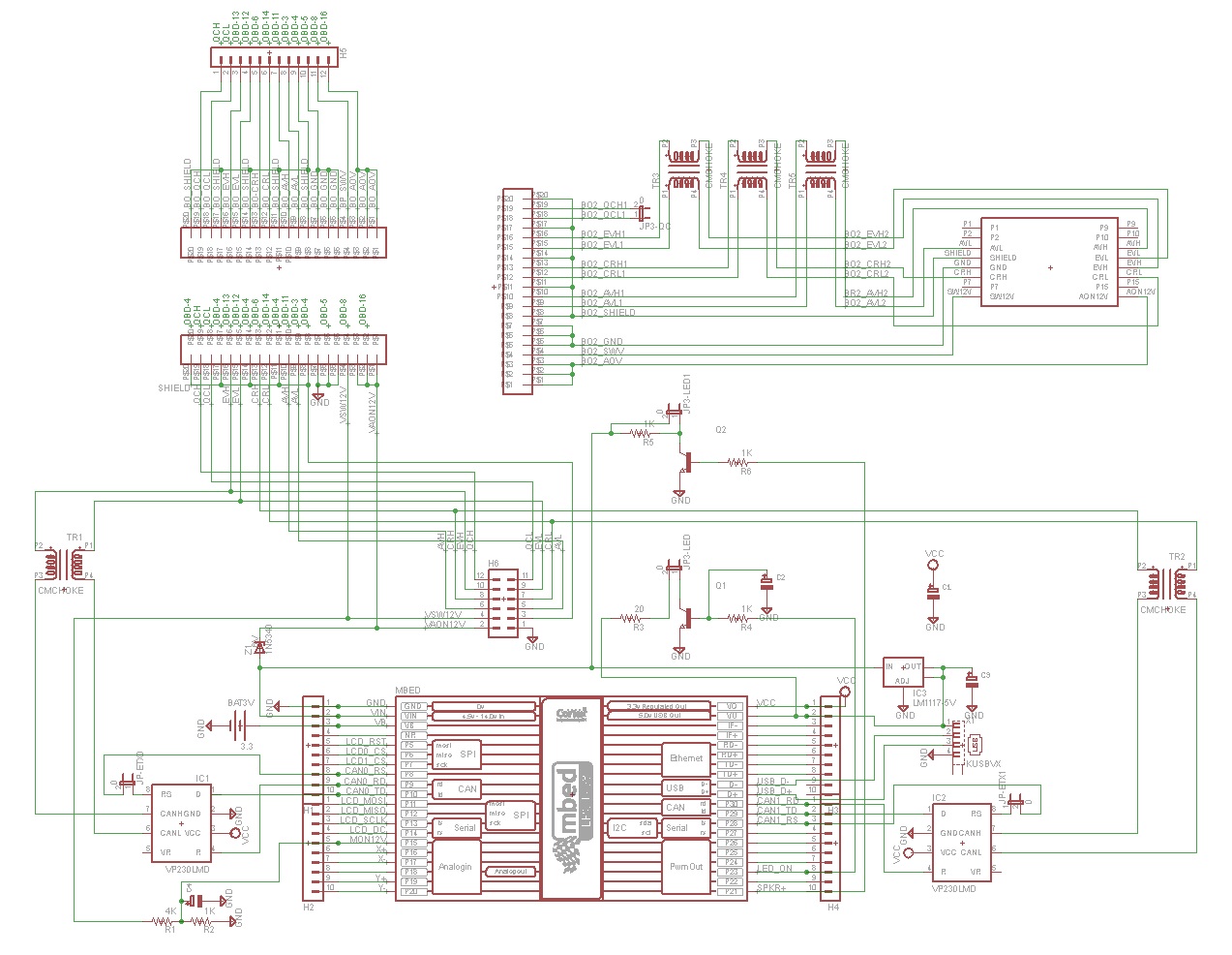
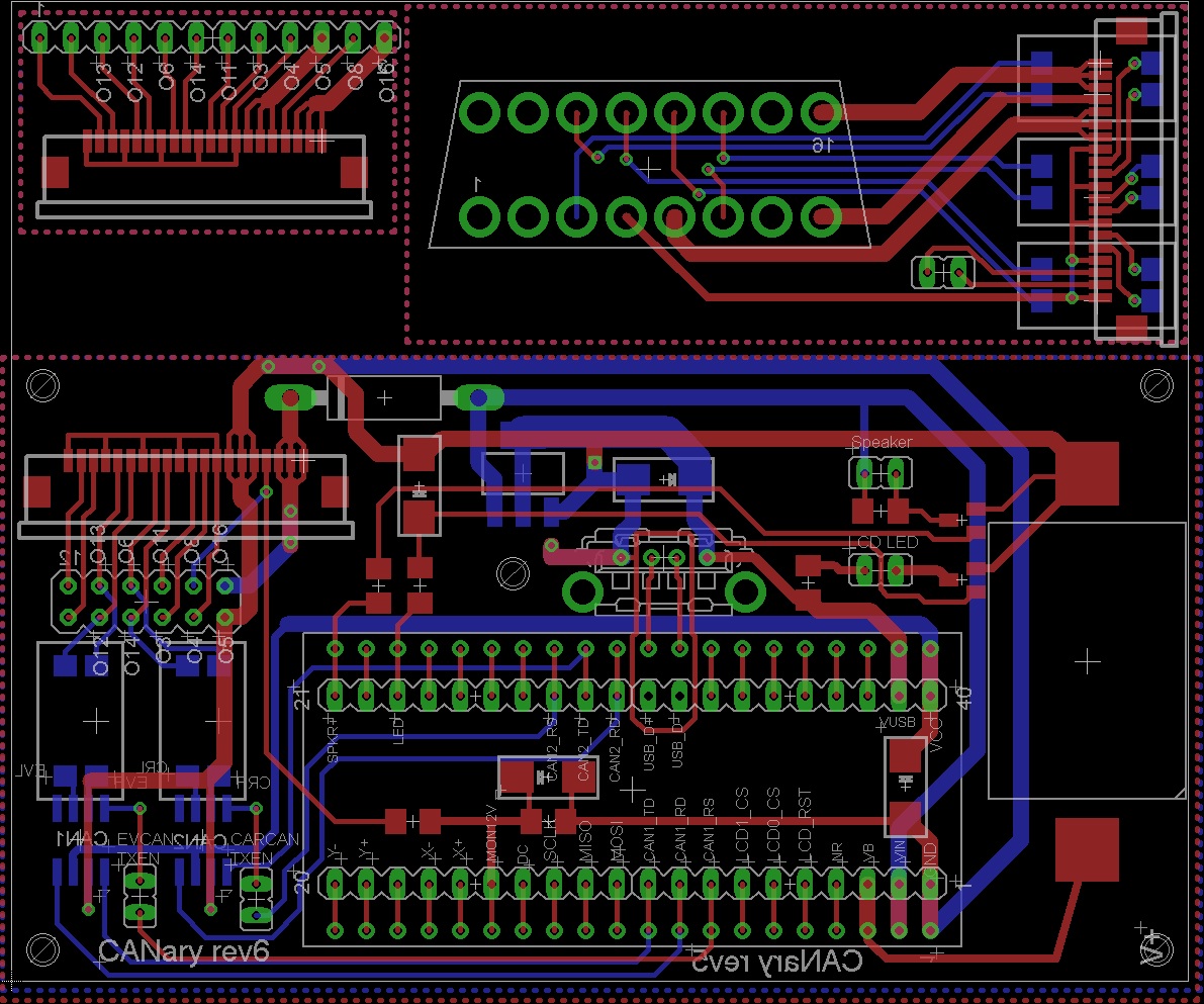
Eagle Schematic and Board design
/media/uploads/TickTock/canaryr6.zip
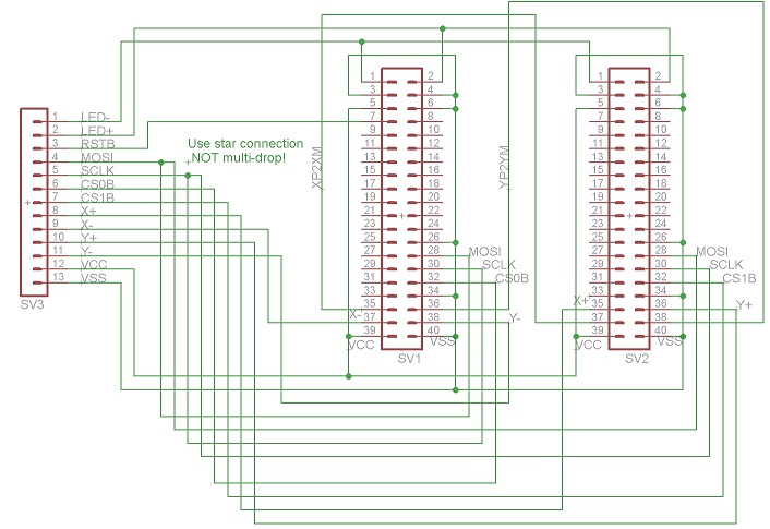
For LCD Rev 1.01:
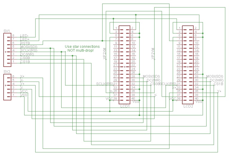
For VCD Rev 2.00:
Parts List
Assembly
1) LCD Displays
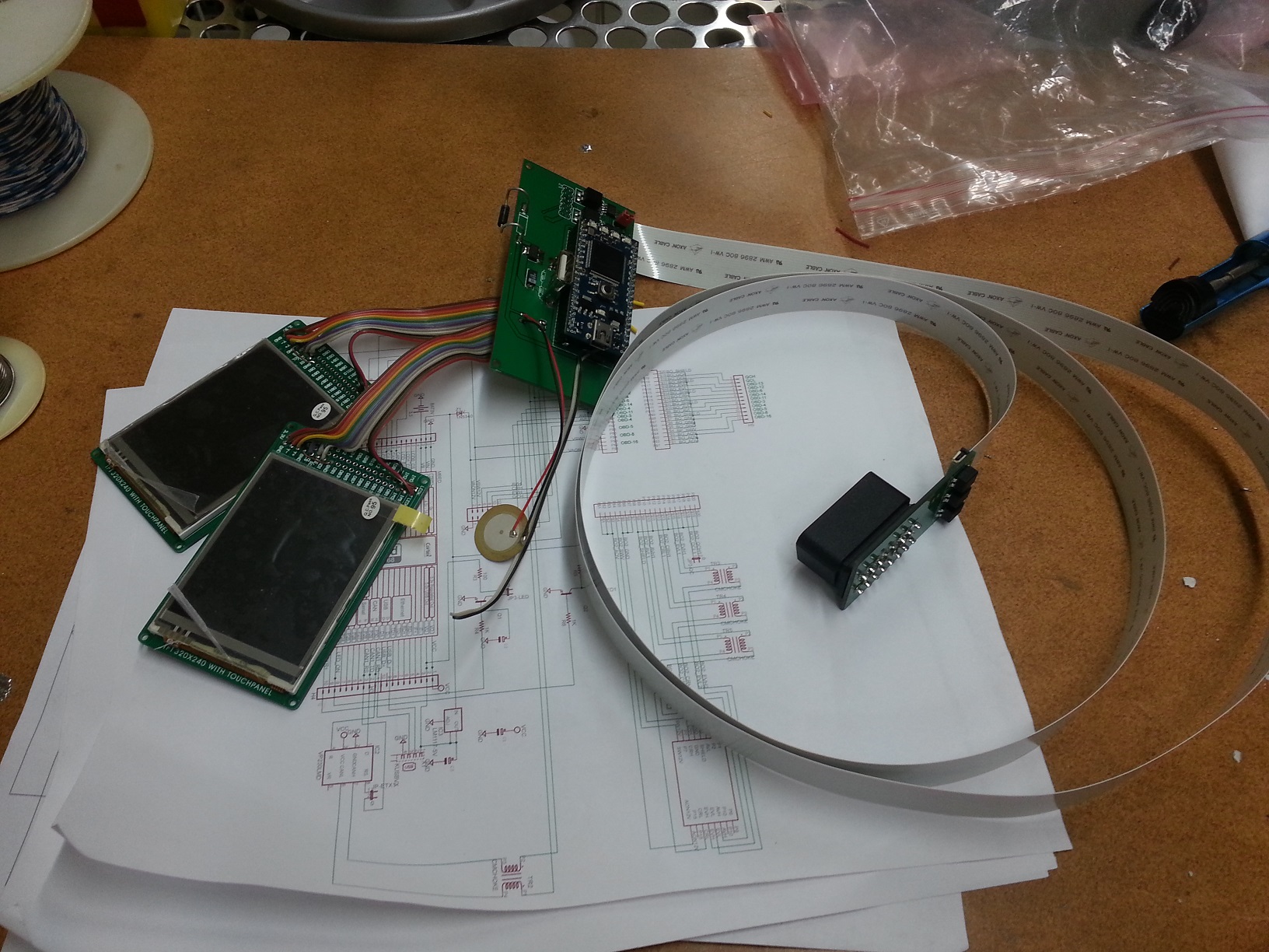
I found ribbon cable is a nice way to organize the wires to the displays. There are two versions of the display and each must be wired differently. The original project used HW REV. 1.01. For that version, you'll need 12 conductors and I connected them in the following order:
| 1 | LED+ |
| 2 | LED- |
| 3 | RST |
| 4 | SDI |
| 5 | WR/SCLK |
| 6 | CS |
| 7 | X+ |
| 8 | X- |
| 9 | Y+ |
| 10 | Y- |
| 11 | VDD |
| 12 | GND |
If, instead, you have HW REV 2.0, you will need 13 conductors with the following order:
| 1 | LED+ |
| 2 | LED- |
| 3 | RST |
| 4 | SDI |
| 5 | RS (SCLK) |
| 6 | WR (DC) |
| 7 | CS |
| 8 | X+ |
| 9 | X- |
| 10 | Y+ |
| 11 | Y- |
| 12 | VDD |
| 13 | GND |
First I connected all the GND connections (2 GND & IM0, IM1, IM3 for REV1.01 or 2 GND, RD, & IM0 for REV2.00). Do not connect the bottom GND until you have the ribbon cable connected. After making all the ribbon cable connections (connecting the GND of the ribbon cable to the bottom GND pad), solder the GND bar from the previous step to the back of the bottom GND connection. Finally, make a connection from the back side 3.3V pin to IM2 for REV1.01 or to IM1,IM2,&IM3 for REV2.00. Take a break and repeat for the second display.
Examples of REV1.01 boards:
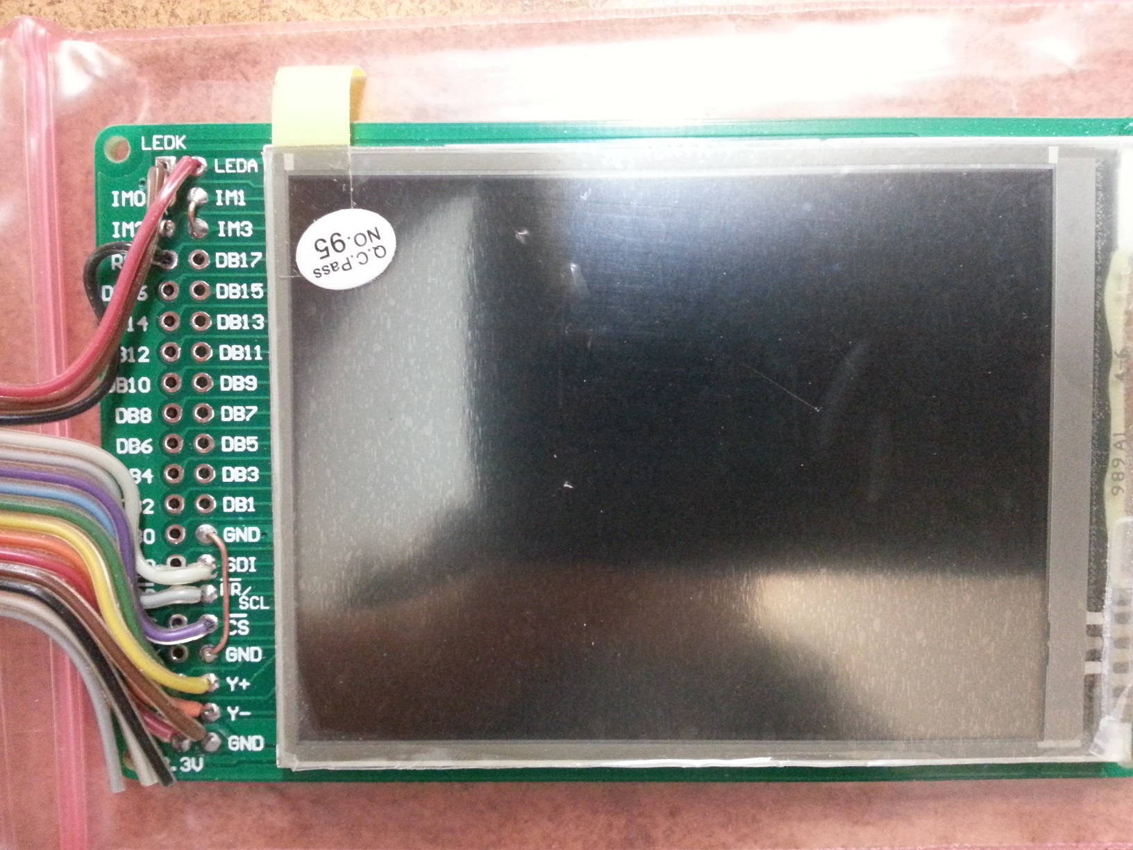
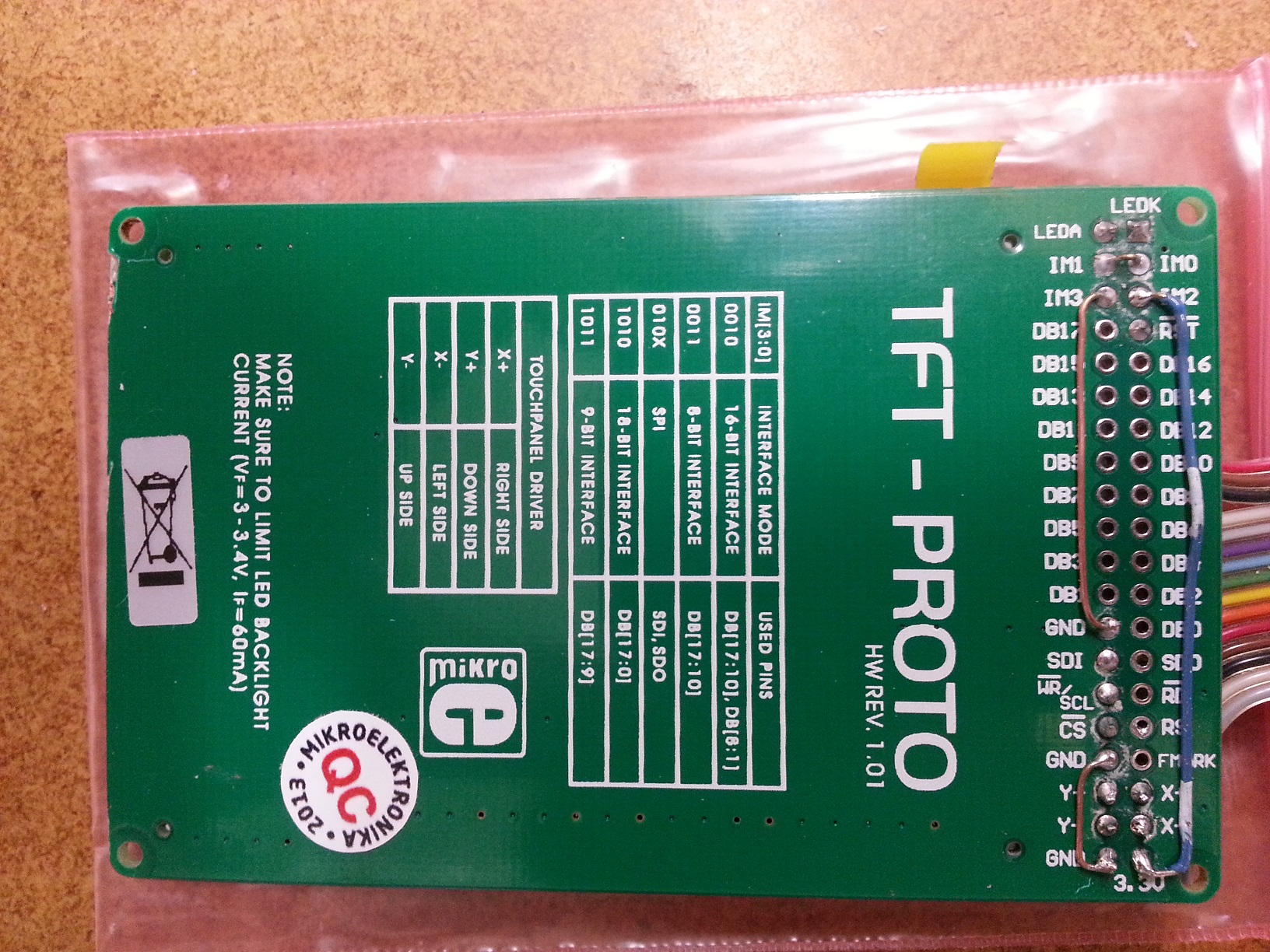
Examples of REV2.00:
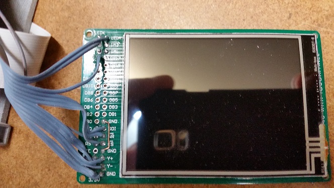
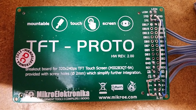
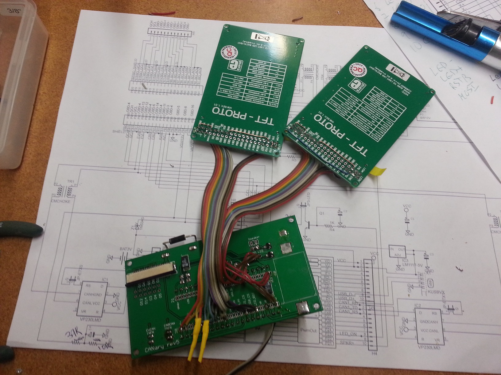
Once the two displays are complete combine all wires except CS0, CS1, X+, X-, Y+, and Y-. Connect X- of the left display to X+ of the right. Similarly connect Y- of the left display to Y+ of the right. Insulate any exposed wires.
2) PCB
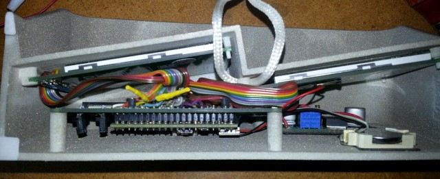
Refer to the schematics to place all the components on the board. If you plan to install into the CANary 3D enclosure, DO NOT install the battery holder or the socket for the mbed and, instead, connect two wires to the VB and GND pads nearby. You will have to install the battery holder against the back wall to avoid interfering with the right-hand display and the mbed will have to be directly soldered. I have not found a socket with a low enough profile to fit in the space provided (depth of enclosure is limited by the space behind the center console). Also, I recommend keeping as much lead as possible on the Zener diode (bending it as shown to clear the back wall). Although it is operating well within parameters, the Zener gets quite hot during extended operation and the leads help dissipate the heat and keep it away from the PCB and other components.Update: Several Zeners have failed resulting in damage to some users boards so I recommend using a DC-DC converter instead to bring the 12V down to 7V.
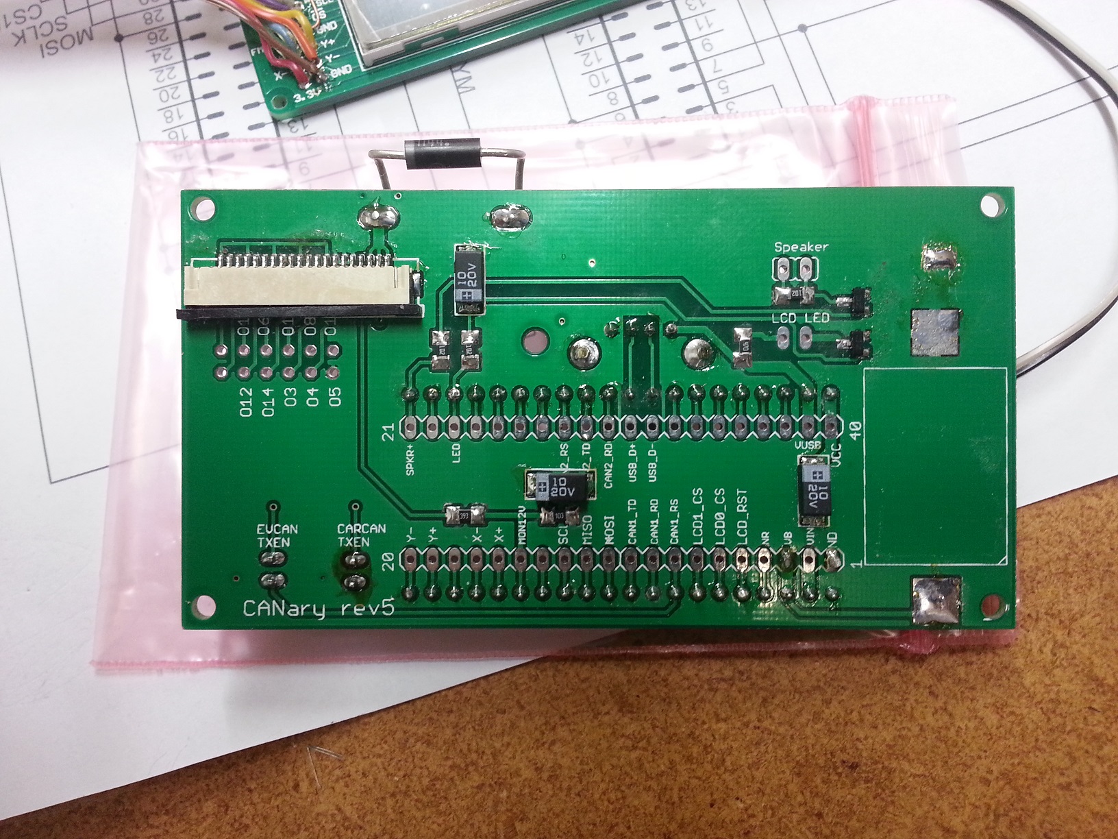
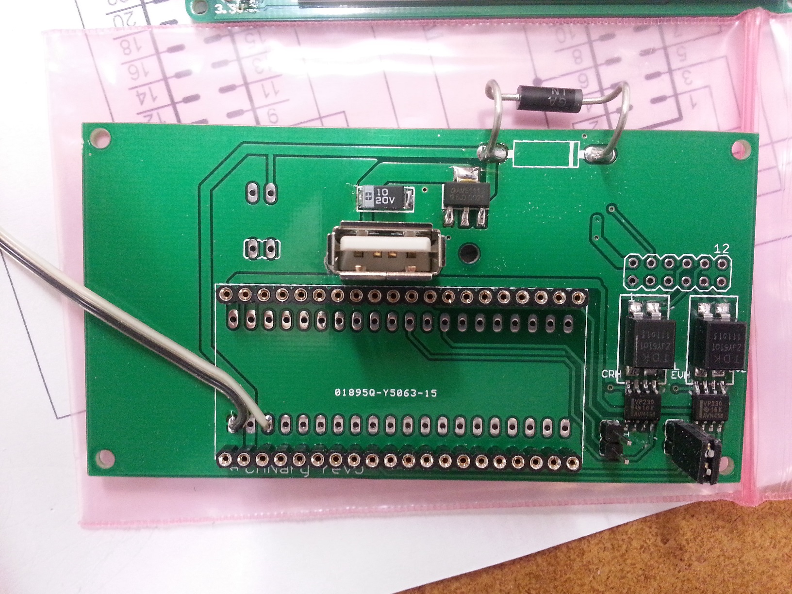
Once the PCB is populated, solder the LCDs to the PCB. CS0 connects to the right display and CS1 connects to the left.
Update:
The Zener diodes tended to fail after a few months so I am recommending removing them and replacing with a DC-DC converter. This will run cooler and waste less energy, too. To install, remove the left display panel to gain access to the Zener. From there, the Zener can be removed and it's pads used to connect to the DC-DC converter. I recommend setting the output voltage on the bench before installing since the trim pot is tricky to reach once installed. Set it to 7V. The input can be connected to the left pad previously occupied by the zener and the output can connect to the right. GND(-) can be connected to the bottom right pad on the 2x6 header below the flex cable connector. Make sure the GND wire lies flat so it doesn't interfere with the connection of the flex cable.
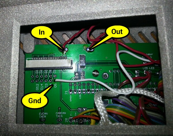
Once soldered in place, the DC-DC converter can easily be mounted to the back wall with double sided tape above the battery holder.
3) Testing
| 1) | First step is to buzz out all connections from the LCDs to the pins in the main board |
| 2) | Next check the touch screen connections. On the main board, place an Ohm meter across X+ and X-. You should read 700 Ohms. Repeat for Y+ and Y-. Then test the resistance from X+ to Y+. With nothing touching the screens, it should read >100K Ohms and <1K when touching either screen. |
| 3) | When all connections are checked, solder in the mbed. Download and install the touch2 program http://mbed.org/users/TickTock/code/touch2/ to test the basic operation of the mbed and touch screens. |
| tips: | |
| Touch screen is sensitive - excess flux on X+,X-,Y+,Y- connection on mbed can result in flakey operation | |
| If touch is not working, double-check the LCD0_CS and LCD1_CS are not swapped. LCD0_CS must connect to the CS of the LCD that has X- & Y- connected to the mbed. LCD1_CS must connect to the CS of the LCD that has X+ & Y+ connected to the mbed. | |
| 4) | Once touch2 works, it is time to connect to the OBD connector. I highly recommend double checking all connections from the OBD to the PCB with the cable in place before connecting to the Leaf. Buzz out all the pins in the OBS to make sure none are shorting to each other, Check that the 12V goes to the Zener (and nothing else) and the switched 12V to the resistor divider (and nothing else). Test the ground connection properly connects to ground and nothing else. |
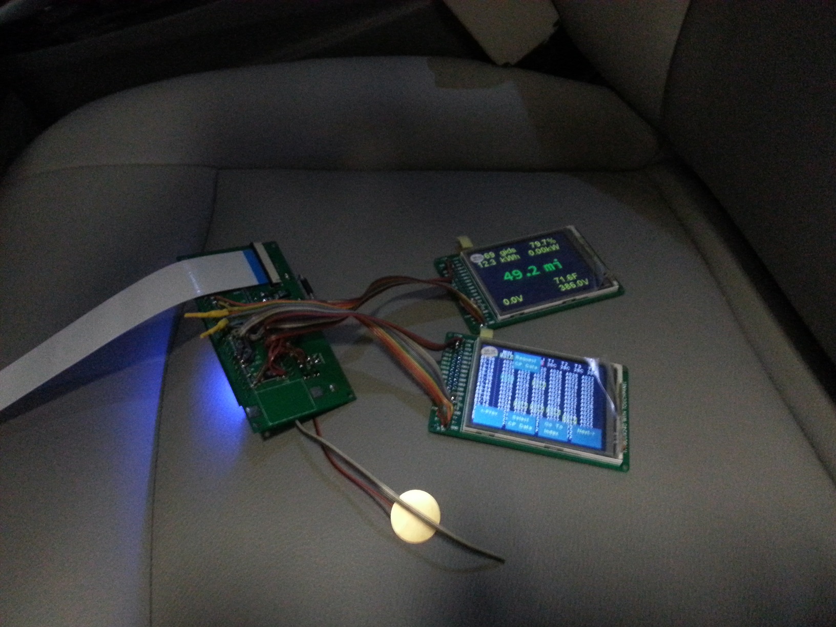
| 5) | Once you are confident there are no shorts or wrong connections from the OBD connector, take a deep breath and plug it into your leaf. Touch2 program should come up and function. Unplug and install the latest CANary firmware. If you have the REV2.00 LCD boards, you will need to edit the precompile.h file in the TOUCH_TFTx2_w9341 library and set USE_ILI9341 to 1. Test all features before installing into the enclosure (gids, cellpair, menu system, logging) since installing and removing from the enclosure is a PITA. |
4) Enclosure
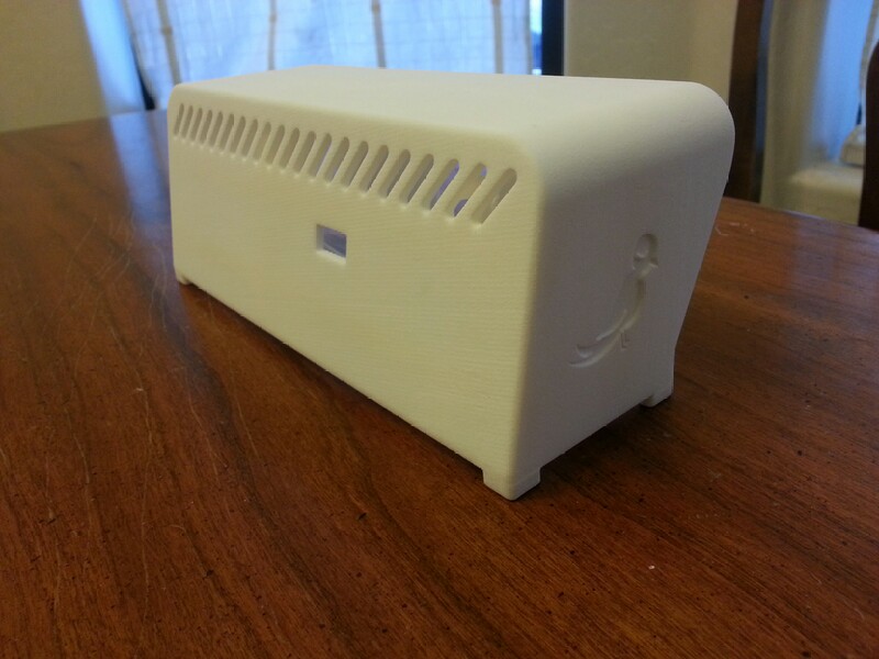
The 3D printer leaves a lot of powder behind - I used a strong spray of water to get it out of all the cracks. The enclosure comes with a rather rough finish. I recommend convincing yourself you like it, then simply lightly sand then paint before assembly. Sanding is very difficult - the nylon is very nicely fused and doesn't want to sand. I tried sandblasting and that didn't work either. I had some limited success with filler and then sanding, but only on the outside - it is too difficult to sand the face.
5) Final Assembly
Make sure you are well rested with lots of patience before attempting assembly. It is a puzzle figuring out how to get both displays and the PCB in place. Enclosure was too expensive for me to keep iterating to optimize for assembly. I ended up snipping the thin display posts shorter and using various tools to push the displays into place. Also, some USB connectors are taller than others. If you have one of the taller ones, you will have to deflect the back wall a bit while inserting the PCB (being careful not to bend the housing) to get it to it's opening in the back wall. Do use a screw in the provided post to secure the PCB as USB insertion will otherwise dislodge it.
I added an additional safety line which wraps around the center post to prevent the enclosure from becoming a projectile in the event of an accident.
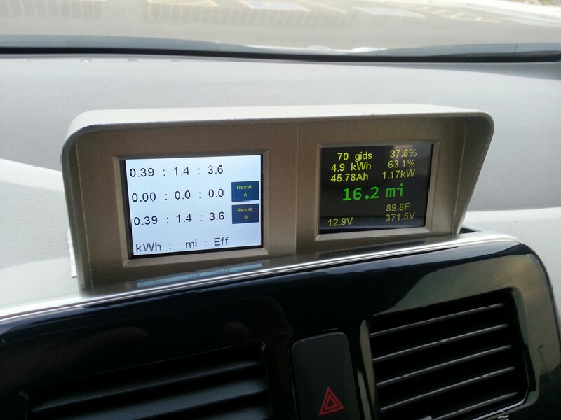
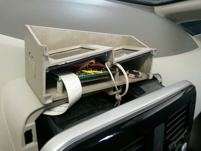 Installed:
PowerControl/PowerControl.h
- Committer:
- TickTock
- Date:
- 2015-07-01
- Revision:
- 208:bfb6b68d1677
- Parent:
- 4:8d7759f4fe7a
File content as of revision 208:bfb6b68d1677:
/* mbed PowerControl Library
  * Copyright (c) 2010 Michael Wei
  */

#ifndef MBED_POWERCONTROL_H
#define MBED_POWERCONTROL_H

//shouldn't have to include, but fixes weird problems with defines
#include "LPC1768/LPC17xx.h"

//System Control Register
// bit 0: Reserved
// bit 1: Sleep on Exit
#define LPC1768_SCR_SLEEPONEXIT     0x2
// bit 2: Deep Sleep
#define LPC1768_SCR_SLEEPDEEP       0x4
// bit 3: Resereved
// bit 4: Send on Pending
#define LPC1768_SCR_SEVONPEND        0x10
// bit 5-31: Reserved

//Power Control Register
// bit 0: Power mode control bit 0 (power-down mode)
#define LPC1768_PCON_PM0            0x1
// bit 1: Power mode control bit 1 (deep power-down mode)
#define LPC1768_PCON_PM1            0x2
// bit 2: Brown-out reduced power mode
#define LPC1768_PCON_BODRPM         0x4
// bit 3: Brown-out global disable
#define LPC1768_PCON_BOGD           0x8
// bit 4: Brown-out reset disable
#define LPC1768_PCON_BORD           0x10
// bit 5-7 : Reserved
// bit 8: Sleep Mode Entry Flag
#define LPC1768_PCON_SMFLAG         0x100
// bit 9: Deep Sleep Entry Flag
#define LPC1768_PCON_DSFLAG         0x200
// bit 10: Power Down Entry Flag
#define LPC1768_PCON_PDFLAG         0x400
// bit 11: Deep Power Down Entry Flag
#define LPC1768_PCON_DPDFLAG        0x800
// bit 12-31: Reserved

//"Sleep Mode" (WFI).
inline void Sleep(void)
{
    __WFI();
}

//"Deep Sleep" Mode
inline void DeepSleep(void)
{
   SCB->SCR |= LPC1768_SCR_SLEEPDEEP;
   __WFI();
}

//"Power-Down" Mode
inline void PowerDown(void)
{
   SCB->SCR |= LPC1768_SCR_SLEEPDEEP;
   LPC_SC->PCON &= ~LPC1768_PCON_PM1;
   LPC_SC->PCON |= LPC1768_PCON_PM0;
   __WFI();
   //reset back to normal
  LPC_SC->PCON &= ~(LPC1768_PCON_PM1 | LPC1768_PCON_PM0);
}

//"Deep Power-Down" Mode
inline void DeepPowerDown(void)
{
   SCB->SCR |= LPC1768_SCR_SLEEPDEEP;
   LPC_SC->PCON |= LPC1768_PCON_PM1 | LPC1768_PCON_PM0;
   __WFI();
   //reset back to normal
  LPC_SC->PCON &= ~(LPC1768_PCON_PM1 | LPC1768_PCON_PM0);
}

//shut down BOD during power-down/deep sleep
inline void BrownOut_ReducedPowerMode_Enable(void)
{
    LPC_SC->PCON |= LPC1768_PCON_BODRPM;
}

//turn on BOD during power-down/deep sleep
inline void BrownOut_ReducedPowerMode_Disable(void)
{
    LPC_SC->PCON &= ~LPC1768_PCON_BODRPM;
}

//turn off brown out circutry
inline void BrownOut_Global_Disable(void)
{
    LPC_SC->PCON |= LPC1768_PCON_BOGD;
}

//turn on brown out circutry
inline void BrownOut_Global_Enable(void)
{
    LPC_SC->PCON &= !LPC1768_PCON_BOGD;
}

//turn off brown out reset circutry
inline void BrownOut_Reset_Disable(void)
{
    LPC_SC->PCON |= LPC1768_PCON_BORD;
}

//turn on brown outreset  circutry
inline void BrownOut_Reset_Enable(void)
{
    LPC_SC->PCON &= ~LPC1768_PCON_BORD;
}
//Peripheral Control Register
// bit 0: Reserved
// bit 1: PCTIM0: Timer/Counter 0 power/clock enable
#define LPC1768_PCONP_PCTIM0        0x2
// bit 2: PCTIM1: Timer/Counter 1 power/clock enable
#define LPC1768_PCONP_PCTIM1        0x4
// bit 3: PCUART0: UART 0 power/clock enable
#define LPC1768_PCONP_PCUART0       0x8
// bit 4: PCUART1: UART 1 power/clock enable
#define LPC1768_PCONP_PCUART1       0x10
// bit 5: Reserved
// bit 6: PCPWM1: PWM 1 power/clock enable
#define LPC1768_PCONP_PCPWM1        0x40
// bit 7: PCI2C0: I2C interface 0 power/clock enable
#define LPC1768_PCONP_PCI2C0        0x80
// bit 8: PCSPI: SPI interface power/clock enable
#define LPC1768_PCONP_PCSPI         0x100
// bit 9: PCRTC: RTC power/clock enable
#define LPC1768_PCONP_PCRTC         0x200
// bit 10: PCSSP1: SSP interface 1 power/clock enable
#define LPC1768_PCONP_PCSSP1        0x400
// bit 11: Reserved
// bit 12: PCADC: A/D converter power/clock enable
#define LPC1768_PCONP_PCADC         0x1000
// bit 13: PCCAN1: CAN controller 1 power/clock enable
#define LPC1768_PCONP_PCCAN1        0x2000
// bit 14: PCCAN2: CAN controller 2 power/clock enable
#define LPC1768_PCONP_PCCAN2        0x4000
// bit 15: PCGPIO: GPIOs power/clock enable
#define LPC1768_PCONP_PCGPIO        0x8000
// bit 16: PCRIT: Repetitive interrupt timer power/clock enable
#define LPC1768_PCONP_PCRIT         0x10000
// bit 17: PCMCPWM: Motor control PWM power/clock enable
#define LPC1768_PCONP_PCMCPWM       0x20000
// bit 18: PCQEI: Quadrature encoder interface power/clock enable
#define LPC1768_PCONP_PCQEI         0x40000
// bit 19: PCI2C1: I2C interface 1 power/clock enable
#define LPC1768_PCONP_PCI2C1        0x80000
// bit 20: Reserved
// bit 21: PCSSP0: SSP interface 0 power/clock enable
#define LPC1768_PCONP_PCSSP0        0x200000
// bit 22: PCTIM2: Timer 2 power/clock enable
#define LPC1768_PCONP_PCTIM2        0x400000
// bit 23: PCTIM3: Timer 3 power/clock enable
#define LPC1768_PCONP_PCQTIM3       0x800000
// bit 24: PCUART2: UART 2 power/clock enable
#define LPC1768_PCONP_PCUART2       0x1000000
// bit 25: PCUART3: UART 3 power/clock enable
#define LPC1768_PCONP_PCUART3       0x2000000
// bit 26: PCI2C2: I2C interface 2 power/clock enable
#define LPC1768_PCONP_PCI2C2        0x4000000
// bit 27: PCI2S: I2S interface power/clock enable
#define LPC1768_PCONP_PCI2S         0x8000000
// bit 28: Reserved
// bit 29: PCGPDMA: GP DMA function power/clock enable
#define LPC1768_PCONP_PCGPDMA       0x20000000
// bit 30: PCENET: Ethernet block power/clock enable
#define LPC1768_PCONP_PCENET        0x40000000
// bit 31: PCUSB: USB interface power/clock enable
#define LPC1768_PCONP_PCUSB         0x80000000

//Powers Up specified Peripheral(s)
inline unsigned int Peripheral_PowerUp(unsigned int bitMask)
{
    return LPC_SC->PCONP |= bitMask;
}

//Powers Down specified Peripheral(s)
inline unsigned int Peripheral_PowerDown(unsigned int bitMask)
{
    return LPC_SC->PCONP &= ~bitMask;
}

//returns if the peripheral is on or off
inline bool Peripheral_GetStatus(unsigned int peripheral)
{
    return (LPC_SC->PCONP & peripheral) ? true : false;
}

#endif
