Mbed design of analog part

05 Dec 2010 . Edited: 06 Dec 2010

Hi all,

One of the main reasons I started with the Mbed is the availlability of the on-board AD converter. I already posted another topic about this. My experiences show that the analog part of the mbed design is not one of the best.

Today I started to experiment a little bit with it.

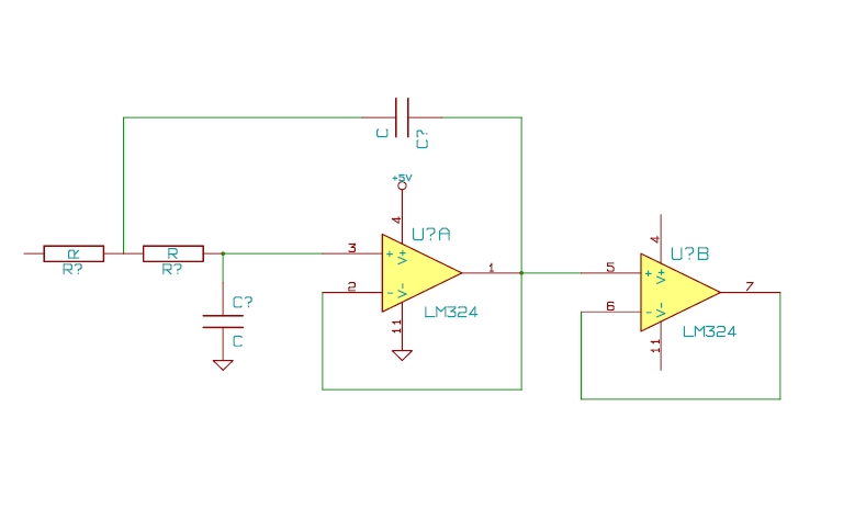
First I made a low pass filter with a buffer, so I wouldn't influence the output signal with the input impedance of the Mbed. Simple design, nothing fancy. Power source external +5V.

On the input is a pressure sensor MPXS 4100 connected. Yes I know, there are digital sensors with A/D conversion in it. But I want to connect more analog signals.

Resistors are 15k, capacitors are 10 nF, cutoff frequency is 1 kHz.

I checked the output signal of the second OpAmp with an oscilloscope, 2 mV/div, looks normal:

After that I connected the output of the second opamp to pin 20 of the Mbed and started to sample the signal. Variance > 10% in the measurements.

I connected the scope again on the output signal of the second OpAmpl with this result, still 2 mV/div:

After disconnecting pin 20 of the mbed the signal is again like the first image from the scope. So I connected the scope to pin 20 without anything else (open pin). Result (5 mV/div):

Since it is an open pin, this can happen. So I pulled it down to ground with a 1k resistor. Same signal as in the second scope image.

The resolution of the AD converter is  3.3 / 2^12, so appr. 0.8 mV. The signal I measured is 8 mV, or appr. 10% of the resolution, which is consistent with my measurements.

So mbed guys, is there a design error in the analog part of the board?

07 Dec 2010

Hi all,  Hello Mario,

I am also having difficulties with the AnalogIn. As a simplest test I could think of, I connected the D/A output, pin 18, to an A/D input. Inputs AD0.2 and AD0.4 are really close by (pin 17 and 19) and can be conveniently connected using a jumper, like this:
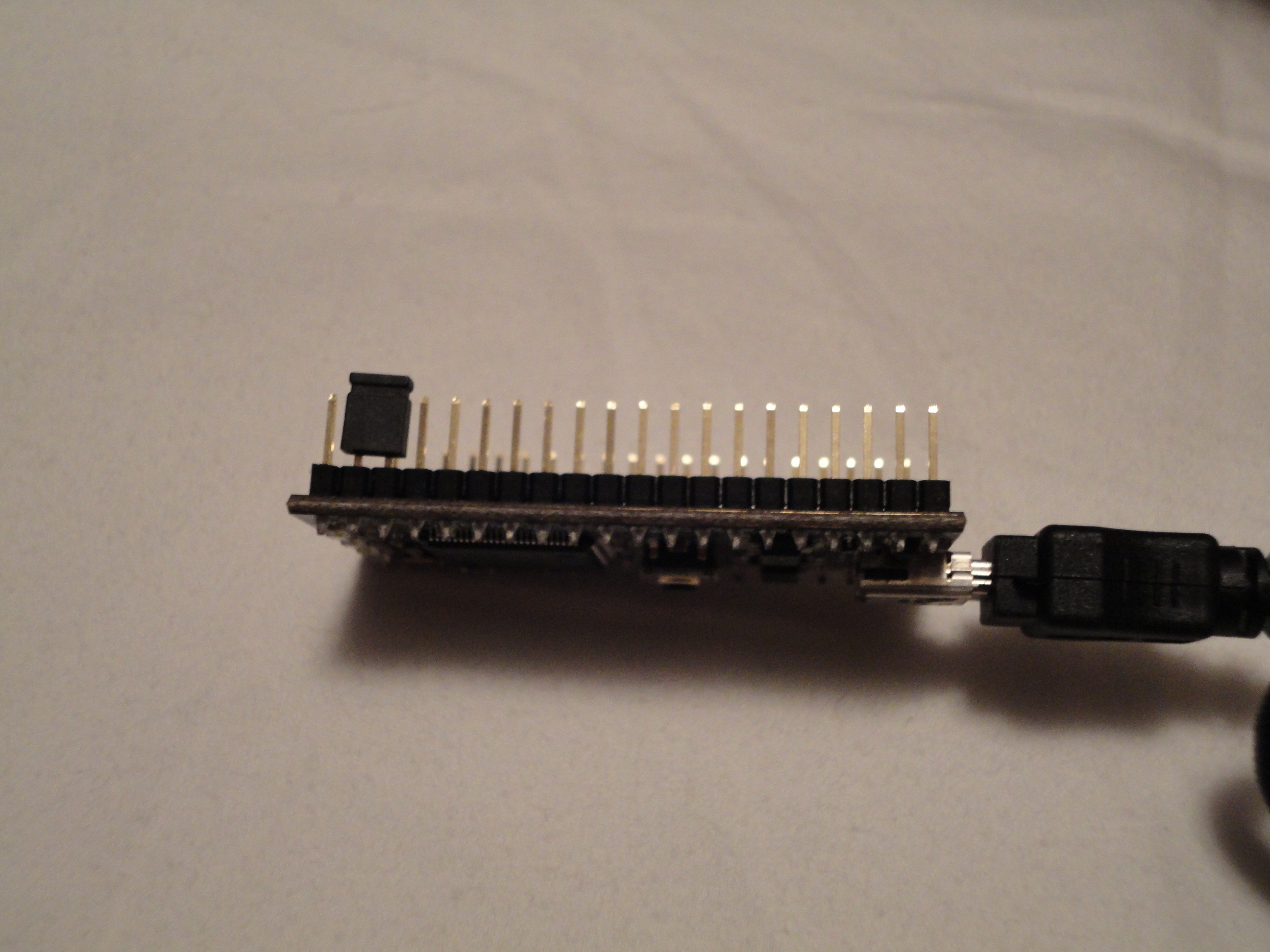
(Here it is pin 18 & pin19.)

The jumper can be pushed all the way down onto the pins. This makes for a very short connection, minimizing capacitive or inductive coupling to other sources besides the analog output. It also avoids connecting to digital ground or supply voltages.

It is then a simple matter to scan through all the 1024 D/A values and for each one of these acquire a set of A/D readings, for instance with a program like this:

dacadctodiskshort

The resulting binary file can be analyzed in various ways, for instance, using matlab:


fh=fopen('d:\out.txt','r');
d=fread(fh,[200,1024],'uint16');
fclose(fh);
d=floor(d/16)';
plot(d,'b.'); axis tight

The last line plots all the data points. For pin 17 on my mbed, the result looks as follows:
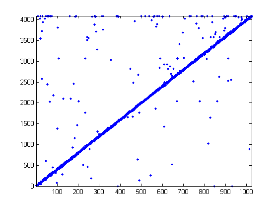
Most of the values are on the line y=4x, as one would expect for a 10 bit D/A and a 12 bit A/D, but unfortunately, there are quite a few points that do not seem to have been converted well by the A/D.  And the bad news is that these are not just all 0x000 or 0xFFF, so it is hard to reject them programmatically.

Interestingly, the 'misconversions' do not seem to come completely randomly, as can be shown using the following:

m=0:1023;
m=repmat(m'*4,1,size(d,2));
imagesc(d'-m',[-30 30])
colorbar
This shows the difference between the measured and expected A/D value as colors:
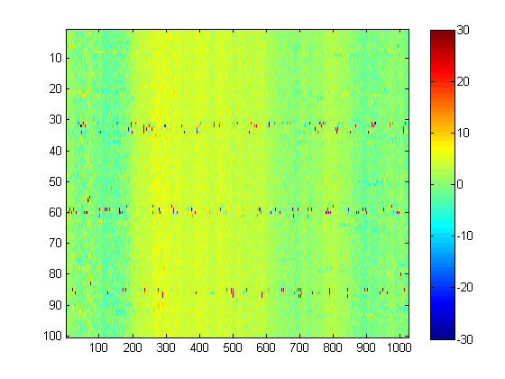
Clearly the misconversions come at more or less regular intervals.

I would be very interested to hear if other people get similar results...


Best regards,

Mischa


07 Dec 2010

I would be intrested to see a graph of input against time. you might be able to do software filtering of the results. I will probably end up looking at  this some time today.

also, it may depend on power supply. try it with the mbed hooked up to a bench power supply, and again with the usb cable. migh also try breadboarding with various capacitors and see what happens.

07 Dec 2010

That's some very nice analasys. What do you mean 'misconversions'. Do you mean the ADC doesn't convert properly or you just aren't getting the value you expect. It looks like noise to me..

See here

07 Dec 2010

Hi Igor,

I'm aware of that. However, to me it doesn't look like noise at all, usually noise affects all the measurements more or less equally. In the observations, most of the measurements are actually spot on (on the line y=4x as expected). You should realize that there are 100x1024 measured data points in the first plot above, and fewer than 150 are off the straight line. Well below 1%. And the ones that are off are off all over the place, not some narrow statistical distribution with a certain variance, as one would expect for Gaussian noise for instance.

I find it hard to stomach to just dismiss this as 'noise'.  If you insist on not blaming the ADC then at least it is more properly characterized as interference. Which would still need to be explained. And the analog input is only connected to analog out via a very short signal path.  No digital supply or ground involved. So where does this come from?

Anyone interested in running my program with pin 17&18 connected? I'll make you a plot if you put up the out.txt somewhere for me to read.

Mischa

07 Dec 2010

Ill run the program later tonight or in the morning.

08 Dec 2010

Hi Christopher,

That would be nice, thanks!

As for the graph of input against time you asked about - there are a bit too many measurements (102400) to really show them all in one figure, that's why I made the second figure above, where time runs from top to bottom first on the left (100 data points) and then proceeds in the 2nd column (next 100 data points, top to bottom) and then the 3rd column, etc.  Basically it is just a ramp from 0 to 1023 on the dac.

As for software filtering: in my experience, just taking an average doesn't help very much since the offending points have such high and low values.  If the input voltage is known to be steady, then a median filter works, but it requires sorting the samples, not very attractive. Unfortunately, if we I want to use the full bandwidth of the ADC, then software filtering cannot save us.

Your suggestion to use a benchtop power supply is interesting since it is easy to try, but note there is 1) a large ferrite bead on the usb cable, 2) a voltage regulator and caps on the mbed pcb, and 3) a filter for the analog supply of the LPC1768. But maybe I trust this too much...

Best,

Mischa

08 Dec 2010 . Edited: 08 Dec 2010

Interference would be the word I should have used. I didn't mean to dismiss your efforts, I just wanted to point out that this has been discussed before.

I am curious, how can you be sure that some of the extraneous points are not because of the D/A converter instead?

08 Dec 2010

Hi Igor,

Of course, I cannot be absolutely sure that the extraneous points are not due to the D/A converter somehow.  But the reason it seems unlikely to me that the D/A converter has much to do with it is that the D/A converter is only reprogrammed once every 100 A/D conversions, and after setting the D/A to a new (and only very slightly different) value, the program waits a little before doing the A/D acquisitions. Hence my presumption that it is not the D/A. Would you agree? Or am I overlooking something?

With kind regards,

Mischa


08 Dec 2010

so I have a set of output files, stored in a public folder on dropbox.

the mbed was put into a breadboard, and shorted using the smallest possible route.

http://dl.dropbox.com/u/8095470/MbedANALOGtest/OUT.TXT

http://dl.dropbox.com/u/8095470/MbedANALOGtest/OUTPSU.TXT

http://dl.dropbox.com/u/8095470/MbedANALOGtest/OUTUSBtiedgnd.TXT

http://dl.dropbox.com/u/8095470/MbedANALOGtest/OUTPSUtiedgnd.TXT

the first is attached to a USB cable and pins 17, 18 shorted.

second is powered from a 5 volt rail, on a bench power supply.

the next two are repeats with the open ADC pins (15,16,19,20) pulled down to ground through 150 ohm resistors(mbed ground pin)

then modifying the code to wait for 0.01 instead of 0.001 after setting the DAC, and using the same setup

http://dl.dropbox.com/u/8095470/MbedANALOGtest/OUTUSBlongwait.TXT

http://dl.dropbox.com/u/8095470/MbedANALOGtest/OUTPSUlongwait.TXT

http://dl.dropbox.com/u/8095470/MbedANALOGtest/OUTUSBtiedgndlongwait.TXT

http://dl.dropbox.com/u/8095470/MbedANALOGtest/OUTPSUtiedgndlongwait.TXT


that should cover issues with power supply, floating input pins on the ADC, and a longer settle time for the DAC.

08 Dec 2010 . Edited: 08 Dec 2010

I did some more experimenting yesterday. It seems that connecting a USB cable to the mbed influences the signal introduced to the analog input pin of the mbed.

No ides if I am the only one that experiences this. Connect an oscillosscope to the analog input pin and see what noise is introduced if the USB cable is attached.

Connecting a capacitor of 10 nF seems to help stabilizing the readings from the ADC.

08 Dec 2010

That makes sense Mischa, I assumed it was a one to one conversion between the D/A and A/D converters.

Christopher, I am having trouble with the text files.. When I open them, I see a bunch of random charcters. Am I missing something?

08 Dec 2010

When working in matlab, they graph nicely. But yes they are a bunch of random charcters. I don't know what the formatting is, but Im guessing they are output as the binary values, as opposed to text. its Mischa's code, I just ran it a few times.

08 Dec 2010

oh ok. the txt extension threw me off..

09 Dec 2010 . Edited: 10 Dec 2010

Hi Igor,  Hello Christopher,

Yes, the files are binary, to save some space on the USB, but I forgot to change the file extension to something more suitable (and '.bin' might not be a very good idea ;)

As promised, here are the graphs. The first one contains all the data with the short (1ms) wait (after writing to the DAC), the second graph contains all the data with the long wait (10 ms):


The legend: files are in the order red/green/blue/magenta, that means: red: power from USB, green: power from power supply; blue: power from USB, other ADC channels grounded; magenta: power from power supply, other channels grounded.

Comparing the graphs and the colors, it becomes clear that using the power supply or grounding the other A/D inputs does not solve our problem right away: there are points of all colors everywhere. It is striking that the upper left triangle appears more densely populated than the lower right triangle in both graphs. Somewhat surprisingly (to me at least) is that the extra waiting time seems to help, in the sense that the second graph appears to have less 'off' points than the first. But the differences are not overwhelming (indeed the green points seem more populous in the lower right triangle of the second graph).

To facilitate a comparison of the various cases, I have made a bar graph, counting the outliers:

From top to bottom: red: A/D values above 4090; yellow: A/D values more than 50 above the expected value (and not red or black); cyan: A/D values more then 50 below the expected value (and not blue or black); blue: A/D values below 6. It is said a picture is worth a thousand words, so here goes:

The matlab script to make these plots is now included withdacadctodiskshort

The bars in the graph above are numbered 0 to 7, again in the order of the files; interpreting the number as 3 bits, this means that bit 2: long wait; bit 1: other inputs grounded; bit 0: power supply.

Comparing the various categories, it seems that the use of a power supply instead of USB has a slightly detrimental rather than a beneficial effect (except in bar 7); similarly, the grounding of the unused A/D inputs does not appear to bring significant relief from outliers. On closer examination, it turns out that grounding the other inputs does have a beneficial effect on the noise (i.e., the width of the line y=4x). I have also found that pin 17 is very different from pin 19. But I'll save the details for next time.

Best,

Mischa

09 Dec 2010

Hi Mario,

Do you connect the 10 nF capacitor just between the output of the opamp and ground?  Or is the opamp not connected, and is it still the 1k resistor?

And about the oscilloscope images: how many microseconds/div are these, do you still have the number somewhere?

Best,

Mischa

09 Dec 2010

Very good work! It's interesting how the bad samples are more often above the actual value. I meant to hook up the scope and try to see if the bad samples actually appear on the pin itself or if they are bad conversions. I'll have a closer look on the weekend. It might take some doing to sync the scope and the mbed properly, I don't know how sucessful I'll be, but it's worth a try..

A few other options worth exploring is to set the AnalogIn pin to PullUp or PullDown and PullNone to see if that has any effect on the conversions. I do not know if the default A/D pin configuration is, I assume its PullNone. We can also try to power down the interface chip. I think that the addition of the ground plane in the other post did wonders. I'll try to rig that up on the weekend, that way we might be able to narrow down the possibilities.

09 Dec 2010

Hi Mischa,

I just connected the 10 NF to the output of the opamp, while it was connected to the input pin of the mbed (p20). Connecting the output of the opamp to the input of the mbed introduces the signal. I will make some scope shots of that this evening, can't do it right now.

Then I can check the horizontal settings of the scopt, I believe it was .5 usec/div

Regards,

Mario

10 Dec 2010

Hi all,

There was a mistake in the count for the red part of the bar graph above, it was overestimating because the high D/A values do result in legitimately high A/D values.  I have corrected the graph and the matlab script that generates these plots from Christopher's data is now included in dacadctodiskshort

Best,

Mischa

10 Dec 2010

Hi

What is the scope time base in the pictures ? Are you seeing the clock frequency ?

11 Dec 2010 . Edited: 11 Dec 2010

To take the DA out of the equation I used a 1.5v D cell as a solid DC reference source.

My Fluke 73 measured 1.605v. I connected the battery via 12" jumper to the AnalogIn pin.

Repeated sampling at 0.001s I get similiar results as described above. Many of the

data points are pegged at the maxium 3.3v.

Placing a 0.01uF ceramic capacitor from the AnalogIn pin to ground, and then

a ferrite bead ( Steward 28C0236-OEW ) from the AnalogIin to the battery jumper

virtually eliminates the instability. I got average readings of 1.612v.

Then I used 2 D cells in series which the Fluke read as 3.207v. I got average readings 3.234v.

---

Reading 16 bit values from the AnalogIn are left justified as expected. The 12 most

significant bits is the actual data. I found that the lower 4 bits is the same as the 4 most

significant bits. So the bottom nibble needs to be zeroed out before using.

read_value &= 0xFFF0;

or

read_value >> 4  // for 12bit values (0-4095)

or

read_value >>6  // for 10bit values (0-1023)

---

For Meshas test of connecting the AnalogOut to the AnalogIn, I found stable results

if I place the ferrite bead between the two pins and then a 0.01uF capacitance from the AnalogIn

pin to ground.

Here is the loop program. I'm printing the results to pc.


    for (i=0;i<1024;i++) {
        j=(i<<6);
        aout.write_u16(j);
        wait(0.001);

        x[0]=ain.read_u16();

        d=abs((x[0]>>6)-i); // just comparing 10 bits out to the 10 bit in

        pc.printf("level out=%d out=%X in=%X in=%X %d err=%d %.3fV \r\n",i,j,x[0],x[0]&0xFFF0,x[0]>>6,d,3.3*(x[0]/65520.));

    }


The err= is the difference between the 10 bit value output to the DA and the value returned

from the AD but limited to 10 bit value. On my mbed I get larger differences for values of  i<140;

around 7. The err for values 500 < i < 1023 is down to 1 to 2.

11 Dec 2010

from the datasheet, http://ics.nxp.com/products/lpc1000/datasheet/lpc1763.lpc1764.lpc1765.lpc1766.lpc1767.lpc1768.lpc1769.pdf pages 61 to 64.

table 18 recomends a resistor between the source and pin of 7.5 Kohm, and a capacitor to ground(Im guessing around 10nF from Mario Raats observation). it also states that the absolute error is 4LSB. so those need to be discounted. I'll modify the experiment, and code to take this into account, and then run the results through Matlab, and compare.

11 Dec 2010 . Edited: 11 Dec 2010

Hi all,

I checked the scope settings, horizontal settings are .05 uSec/div, so the image shows the clock frequency (second picture in first post).

I took another approach. Since I build the electronics on an experiment breed-board, I tried to put it on a "normal" experiment board.

As suggested in the post above, I put in a resistor from 6k8 (couldn't find 7k5 in my collection) and a capacitor of 10 nF on the output opamp. Schematics:


The output goes with 2 twisted wires to pin 20 and ground from the mbed.

I did 1000 samples and wrote the values to a text file on the mbed, and inserted them into an Excell sheet.

Result:

The values on the left are the floats that the AnalogIn function returns. Not bad.

Looking at the values returned, I discovered that 1 step in the ADC was equivalent to a number of 0.000244. That was helpfull in calculating the digital steps from the float. The biggest variance in the digitizing proces was 16 steps, or 0.4% (16 / 4096 * 100%).

11 Dec 2010

Christopher,

That specification means that the maximum source impedences is not to exceed 7.5 Kohm.

There is no minimum source impedence, so zero ohms is O.K.

It does not imply to insert a series resistance. The series resistance and capacitance to ground

shown in the diagram is just the model for the equivalent circuit inside a source such as a battery,

regulator, OpAmp output or other driving circuit.

The goal is to have a low source impendence to reduce noise and input errors.

The 4 LSB absolute error just refers to the maximum uncalibrated error of the 12 bit ADC.

Just want to be clear that is the not the lower 4LSB of the 16bit value that needs to be ignored.

Is the LPC or mbed calibrated at the factory? I don't know. If not, is there a calibration procedure?

I know we can do our own calibration table in our program if needed.

11 Dec 2010
user mario raats wrote:

Hi all,

I checked the scope settings, horizontal settings are .05 uSec/div, so the image shows the clock frequency (second picture in first post).

Hi Mario,

The clock frequency?

Measuring from your oscilloscope image:

I'd say the sharp peaks appear to coincide with the grid lines to better than 1/5 of a minor grid division, i.e., ±0.04 divisions. From this, the observed frequency is

1/((7 ±0.04 div)*0.05us/div /17) = 48.6 ±0.3 MHz, or
1/((9 ±0.04 div)*0.05us/div /22) = 48.9 ±0.2 MHz,
with the assumption that the 0.05us/div is accurate. Perhaps it is time to recalibrate the horizontal scale, if it is 2% out of calibration, then the frequency could be 48.0 MHz.

The mbed crystal frequency is 12 MHz; it uses a PLL to upconvert to 96 MHz (or 72 MHz if you have older firmware; the PLL is programmable). So the frequency that we observe is close to the CPU clock frequency divided by two, or 48 MHz.  This is also the USB clock frequency. That the USB might have something to do with it is consistent with the observation that connecting the USB of the mbed influences the analog signal.

The CPU clock can be programmed independently from the USB clock - that would be a way to independently verify that it is not just the CPU clock divided by two that we are seeing.

Best,
Mischa

11 Dec 2010

Hi all,

user Christopher Hasler wrote:
from the datasheet, http://ics.nxp.com/products/lpc1000/datasheet/lpc1763.lpc1764.lpc1765.lpc1766.lpc1767.lpc1768.lpc1769.pdf pages 61 to 64. table 18 recomends a resistor between the source and pin of 7.5 Kohm,
user Thomas Olson wrote:

Christopher,

That specification means that the maximum source impedences is not to exceed 7.5 Kohm.
There is no minimum source impedence, so zero ohms is O.K.

It does not imply to insert a series resistance. The series resistance and capacitance to ground shown in the diagram is just the model for the equivalent circuit inside a source

I would agree with Thomas that an extra resistor is not required.

Best,
Mischa


11 Dec 2010


user Thomas Olson wrote:
Just want to be clear that is the not the lower 4LSB of the 16bit value that needs to be ignored. Is the LPC or mbed calibrated at the factory? I don't know. If not, is there a calibration procedure? I know we can do our own calibration table in our program if needed.

Hi Thomas,


The 4 lsb of the 16 bit value can be ignored. They are a copy of the 4 msb.  It is the mbed analogin.read_u16() library routine that copies these bits. It has nothing to do with the information in the datasheet whatsoever. It just ensures that the values from the ADC are in the range 0x0-0xFFFF instead of 0x0-0xFFF0, in compliance with the documentation in the handbook at http://mbed.org/handbook/AnalogIn, I suppose.

If you don't like the calibration of your ADC, then you can adjust the value of the ADCOFFS (bits 7:4) in the ADTRIM register, see section 29.5.6 in the LPC17xx user manual. It promises that the register will be set by the bootcode on start-up. It also says that the reset value is 0. The data sheet (above) table18, note 5 says that ADCOFFS should be 2. It appears that changing the ADCOFFS value just shifts he A/D results, as if adding a number proportional to ADCOFFS, where ADCOFFS is a 4 bit binary number in  two's complement (i.e., -8 gives lower readings, 0 gives about the right readings, +7 gives too high readings). You can set is as follows:

short trim = 2; 
LPC_ADC->ADTRM&=~0x00F0;
LPC_ADC->ADTRM|=(trim<<4) & 0x00F0;   //set the trim
Best,
Mischa

12 Dec 2010

Looking at  the  buffer  circuit,  I  think  you  may have a few issues.  Firstly,  you  should not connect a capacitor  straight to the output of an op-amp - and especially an LM324.  It  will oscillate,  and especially soif there is already  some HF noise  around to help it on its way.

Connect the output of the buffer  via a 50 Ohm resistor  to the input to your A-D.  Place a 0.1uF capacitor from the input of the A-D to ground as close to the mBed as possible. I'd even  go for a higher value - like 1uF,  but  of  course  I  don't  know what the  bandwidth  is that you are shooting for  here,  so  this may be a  bit high.

Have  you decoupled the power  supply  pins  of  your  op-amp to ground?  I'd  propose  10uF from each supply pin to GND with 0.1 ceramic  in parallel.  Place thse  componenets as close to the  op-amp as possible.

The LM324 is a slow bipolar op-amp that does not tolerate capacitive  loads  very  well.  If  you are looking for something faster,  let me know  and I'll  propose  some alternatives.

Looking at the  scope  pics,  I also  think  you  have  some serious noise  problems.  However,  with  careful  layout,  a  lot of this can be avoided.  E.g place R4, C1  and the 10nF (cannot read the reference)  as  close to the inverting input of the op-amp as possible - and I  mean within  a few mm.  Any noise coupled between the  junction of these  componenets  and the inverting input is amplifer by the full  loop gain of the op-amp.  Ugly. Same for the second op-amp configured as a buffer - keep the connection between the output the the inverting input short as possible.

Good  luck!


12 Dec 2010 . Edited: 12 Dec 2010

I would say the buffer isn't even needed... The one opamp should be plenty. Heck.. you might even get better results with a passive 2nd order filter if noise is the issue. If you keep the opamps, I would even drop the value of the output resistor even more.. Maybe down to 1k.. or even lower.

12 Dec 2010 . Edited: 12 Dec 2010

Yes,  maybe  a straight 2nd  order  filter  is  the best way to go - no op-amps at  all.