Important changes to forums and questions
All forums and questions are now archived. To start a new conversation or read the latest updates go to forums.mbed.com.
Mbed design of analog part
Topic last updated 20 Aug 2011, by  Paulo Marques.
48
replies
Paulo Marques.
48
replies
Paulo Marques.
48
replies
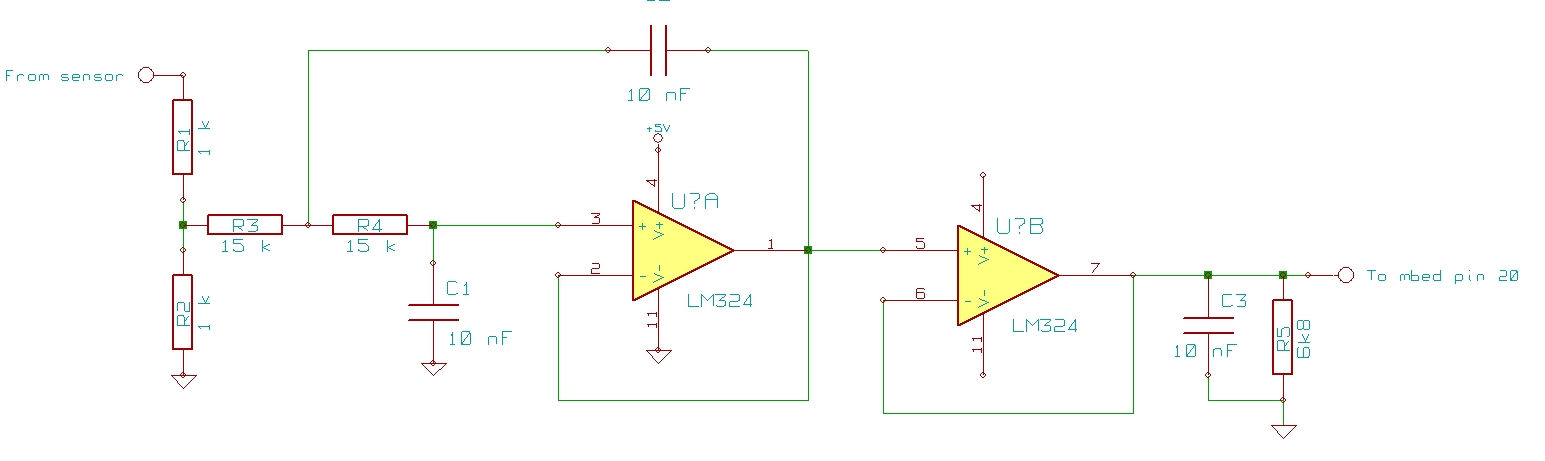
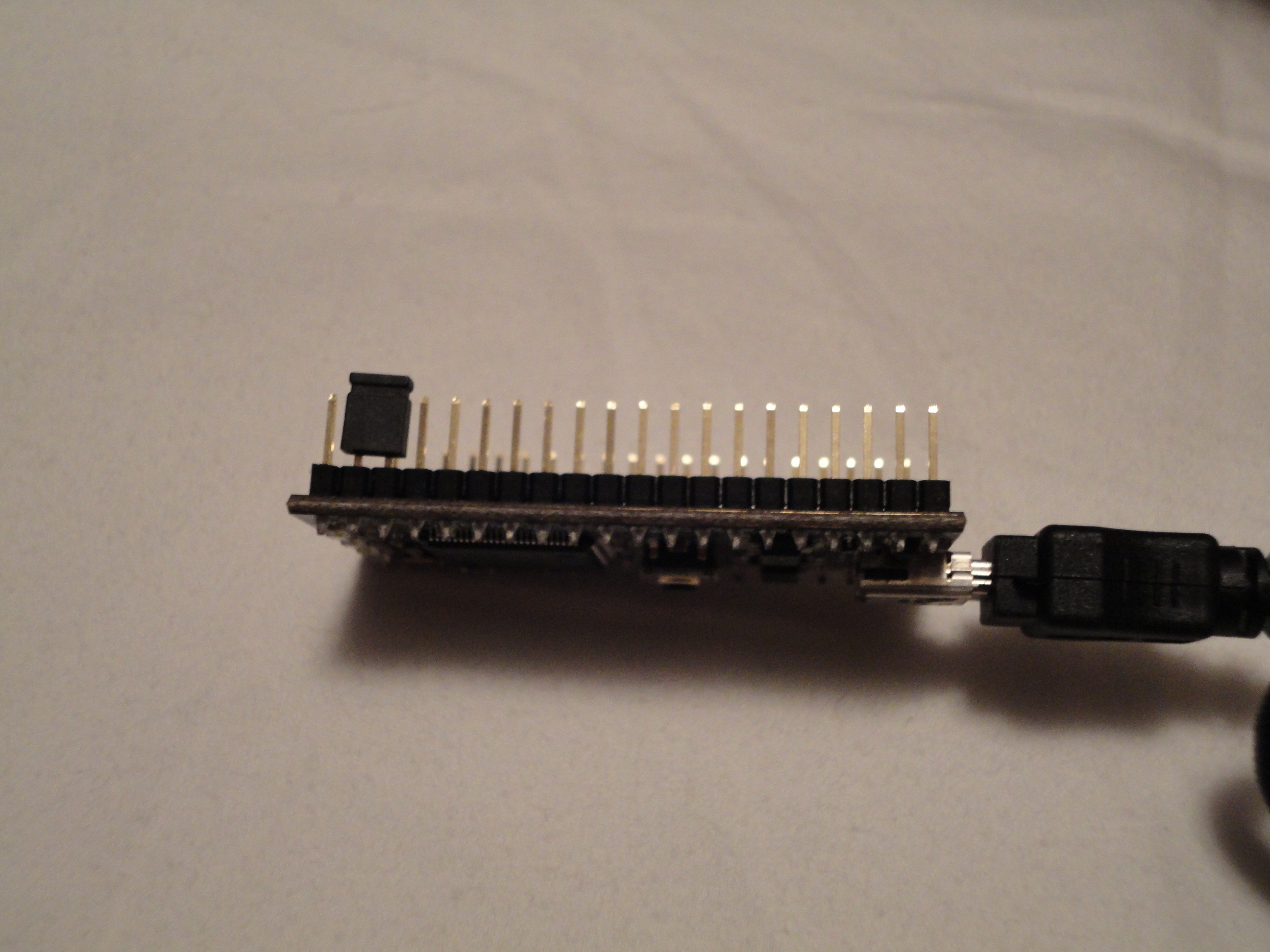 (Here it is pin 18 & pin19.)
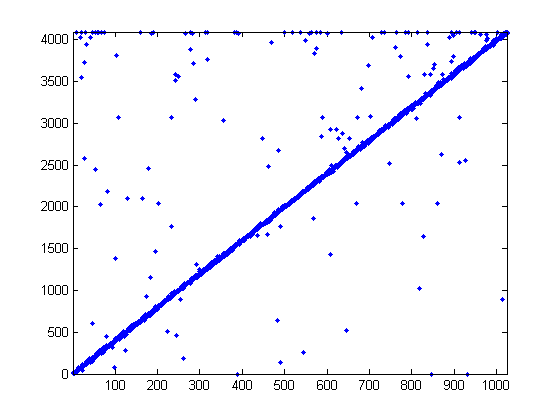


Hi all,
One of the main reasons I started with the Mbed is the availlability of the on-board AD converter. I already posted another topic about this. My experiences show that the analog part of the mbed design is not one of the best.
Today I started to experiment a little bit with it.
First I made a low pass filter with a buffer, so I wouldn't influence the output signal with the input impedance of the Mbed. Simple design, nothing fancy. Power source external +5V.
On the input is a pressure sensor MPXS 4100 connected. Yes I know, there are digital sensors with A/D conversion in it. But I want to connect more analog signals.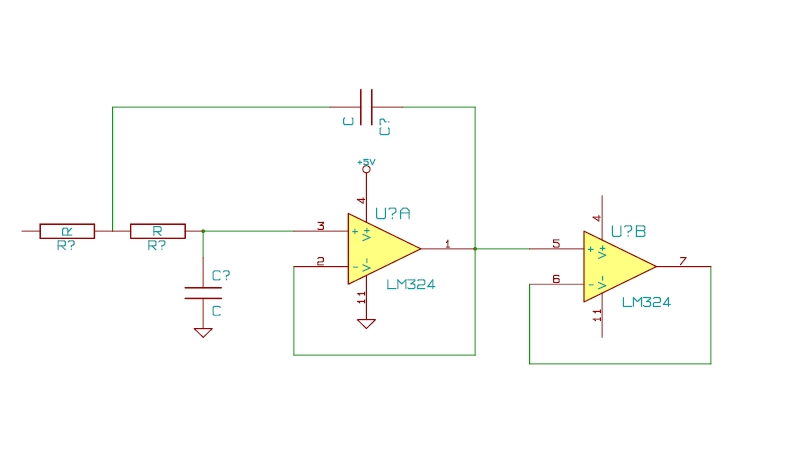
Resistors are 15k, capacitors are 10 nF, cutoff frequency is 1 kHz.
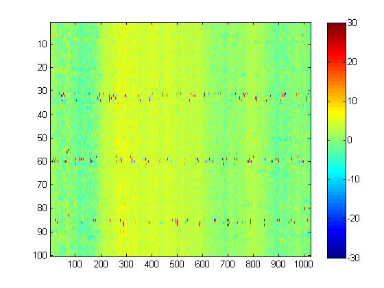
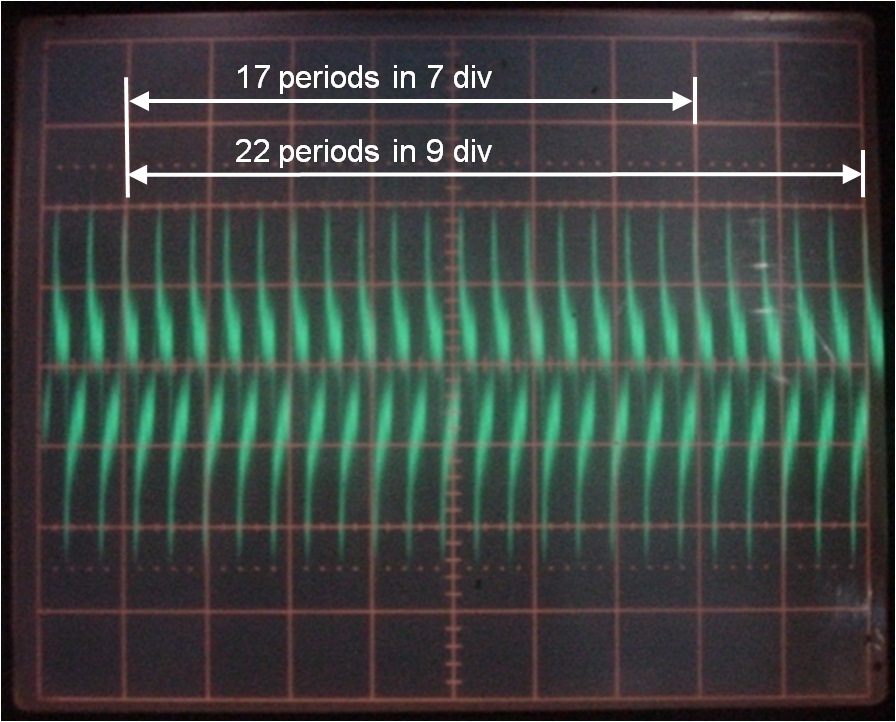
I checked the output signal of the second OpAmp with an oscilloscope, 2 mV/div, looks normal:
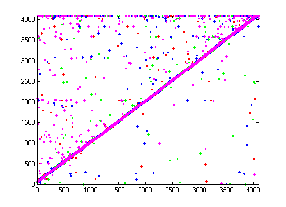
After that I connected the output of the second opamp to pin 20 of the Mbed and started to sample the signal. Variance > 10% in the measurements.
I connected the scope again on the output signal of the second OpAmpl with this result, still 2 mV/div:
After disconnecting pin 20 of the mbed the signal is again like the first image from the scope. So I connected the scope to pin 20 without anything else (open pin). Result (5 mV/div):
Since it is an open pin, this can happen. So I pulled it down to ground with a 1k resistor. Same signal as in the second scope image.
The resolution of the AD converter is 3.3 / 2^12, so appr. 0.8 mV. The signal I measured is 8 mV, or appr. 10% of the resolution, which is consistent with my measurements.
So mbed guys, is there a design error in the analog part of the board?