This post is an extension of the forum thread titled “ADC and DMA” http://mbed.org/forum/mbed/topic/1798/?page=1. That thread discussed the anomalous behavior of the ADC when read in burst mode, particularly with respect to DMA operation.
Similar issues show up in interrupt or polled operation of the ADC in burst mode. This posting discusses the issue in that context.
Recap of the Problem
The problem, as reported by user Wim van der Vegt, is that one cannot rely on correct association of channel number and data value when data is read from the ADGDR “global data register” in burst mode.
Andy Kirkham confirmed that the values read via DMA were off by one index count. For example the first data retrieved should have been channel 0, but was identified as channel 1 by the CHN bits. The ADC result value, however, was correct – it matched the voltage being applied to Input 0 of the ADC.
After further investigation, Andy concluded that the CHN bits were not latched, and thus were showing the currently-converting channel information.
One suggested work-around was to switch to an interrupt-based handler, and have it read the specific ADDR “data register” for each of the burst channels. This avoids the problem with the ADGDR.
The other suggested work-around was to use a channel correction factor if using DMA, which, of course, must use the ADGDR as its source of data.
Further Investigation
I set up a simple series of tests to profile the behavior of the bits in the ADGDR register. The approach was to take snapshots of the register contents at regular intervals, and observe the changes over time.
The contents of the ADGDR register were not processed in any way, but simply saved into an array. An mbed Timer was read immediately after the ADGDR register was polled, and its value also saved into an array.
After the desired number of entries were collected, an output routine read the arrays and sent “printf” data to the pc, for collection by a terminal program. That data was then imported to Excel and plotted.
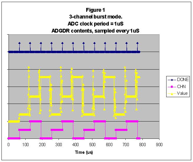
The first plot below shows normal operation of the ADC. The ADC clock was set to 1 uS (CLKDIV = 23). The data samples were taken every 1 uS as well. The ADC was set up to convert channels 0 – 2 in burst mode. The signals applied to the inputs were about 0.38, 1.4, and 2.5 volts for channels 0 to 2, respectively.
The top trace of the graph shows the state of the DONE bit. It is raised approximately every 65 uS (recall that the ADC takes 65 clocks to do a conversion).
The bottom trace shows the CHN field, which counts in sequence 0, 1, 2, 0, 1, 2, and so on.
The middle trace shows the data value at each sample point. The operation of the ADC approximation controller shows up as “oscillation” in the value before the final result is reached. This is expected behavior.

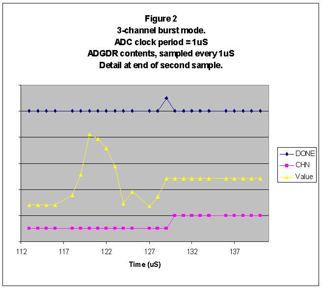
The second plot shows a detailed area around the time that the second sample finishes its conversion. The middle trace shows the data value convergence, the top trace shows DONE rising once data is stable, and the lower trace shows CHN being incremented after DONE is raised. Again, this is expected behavior.

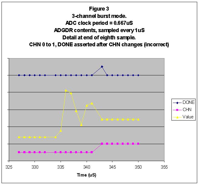
The results so far are well behaved because the ADC is operating with a slow, 1 MHz clock. Problems show up as the speed of the clock is increased. The third plot shows an example of the problem.
Here the ADC clock period has been sped up modestly to 0.667 uS (1.50 MHz). CLKDIV equals 15 for this case. This time the plot of detailed area around the end of the eighth bit shows the proverbial smoking gun: DONE is asserted with the wrong (the new) CHN value. This explains the channel offset mentioned in the introduction.

Speed limit
The fact that the problem gets worse with a faster ADC clock suggests a race condition. I decided to expand the timing for a final test.
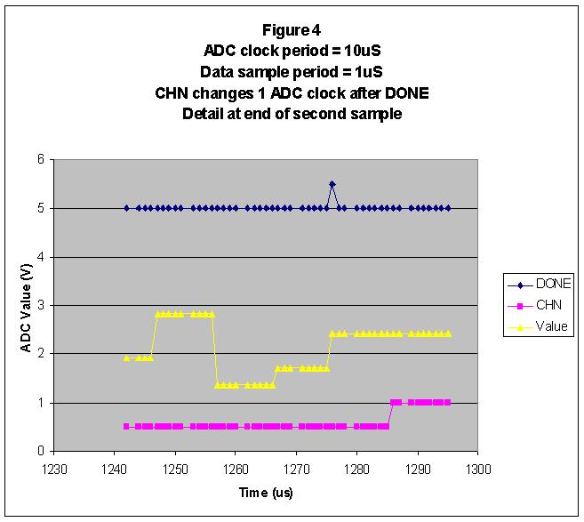
In this test, the ADC clock was slowed way down. I chose a 10uS period (CLKDIV = 239). This would allow my test program to sample ADGDR 10 times during every ADC clock period. I added a delay at the start of the test, so that only data around the end of a conversion would be sampled.
The plot below shows the results. The middle trace shows the ADC value converging on its final value, with intermediate results taking about 10 sample periods as expected. At 1276 uS, DONE is raised. The CHN bits still reflect the proper value.
At 1286 uS, the CHN bits increment. This confirms that they automatically change one ADC clock period after the previous conversion completes.

Conclusions
The ADC allows the user one ADC clock period to read valid data from the ADGDR result register. If more time than that elapses, the data will no longer be valid. The first thing to change is the CHN bits, as shown immediately above. Much later, the data value will bobble about (for the final 12 clocks before the conversion ends).
This means that the latency in the routines that service the ADGDR must be much less than one ADC clock period. Consider what that means. The maximum clock speed is specified as 13 MHz. That gives a whopping 77nS to service the ADC.
Andy K. reported that the DMA could support an 8 MHz clock – so its response time must be better than 125nS. Impressive.
Software polling will only work for slow ADC clock rates. That may not be an issue for quasi-static applications (polling temperature sensors, perhaps). Otherwise, one needs to use something like Simon Blandford’s interrupt-driven approach to burst mode support, which avoids use of the ADGDR altogether http://mbed.org/users/simonb/programs/ADC_test/5zlnn/.
I’m not sure this is a bug (could be just a lack of clear documentation), but it certainly doesn’t smell like a feature.
This post is an extension of the forum thread titled “ADC and DMA” http://mbed.org/forum/mbed/topic/1798/?page=1. That thread discussed the anomalous behavior of the ADC when read in burst mode, particularly with respect to DMA operation.
Similar issues show up in interrupt or polled operation of the ADC in burst mode. This posting discusses the issue in that context.
Recap of the Problem
The problem, as reported by user Wim van der Vegt, is that one cannot rely on correct association of channel number and data value when data is read from the ADGDR “global data register” in burst mode.
Andy Kirkham confirmed that the values read via DMA were off by one index count. For example the first data retrieved should have been channel 0, but was identified as channel 1 by the CHN bits. The ADC result value, however, was correct – it matched the voltage being applied to Input 0 of the ADC.
After further investigation, Andy concluded that the CHN bits were not latched, and thus were showing the currently-converting channel information.
One suggested work-around was to switch to an interrupt-based handler, and have it read the specific ADDR “data register” for each of the burst channels. This avoids the problem with the ADGDR.
The other suggested work-around was to use a channel correction factor if using DMA, which, of course, must use the ADGDR as its source of data.
Further Investigation
I set up a simple series of tests to profile the behavior of the bits in the ADGDR register. The approach was to take snapshots of the register contents at regular intervals, and observe the changes over time.
The contents of the ADGDR register were not processed in any way, but simply saved into an array. An mbed Timer was read immediately after the ADGDR register was polled, and its value also saved into an array.
After the desired number of entries were collected, an output routine read the arrays and sent “printf” data to the pc, for collection by a terminal program. That data was then imported to Excel and plotted.
The first plot below shows normal operation of the ADC. The ADC clock was set to 1 uS (CLKDIV = 23). The data samples were taken every 1 uS as well. The ADC was set up to convert channels 0 – 2 in burst mode. The signals applied to the inputs were about 0.38, 1.4, and 2.5 volts for channels 0 to 2, respectively.
The top trace of the graph shows the state of the DONE bit. It is raised approximately every 65 uS (recall that the ADC takes 65 clocks to do a conversion).
The bottom trace shows the CHN field, which counts in sequence 0, 1, 2, 0, 1, 2, and so on.
The middle trace shows the data value at each sample point. The operation of the ADC approximation controller shows up as “oscillation” in the value before the final result is reached. This is expected behavior.
The second plot shows a detailed area around the time that the second sample finishes its conversion. The middle trace shows the data value convergence, the top trace shows DONE rising once data is stable, and the lower trace shows CHN being incremented after DONE is raised. Again, this is expected behavior.
The results so far are well behaved because the ADC is operating with a slow, 1 MHz clock. Problems show up as the speed of the clock is increased. The third plot shows an example of the problem.
Here the ADC clock period has been sped up modestly to 0.667 uS (1.50 MHz). CLKDIV equals 15 for this case. This time the plot of detailed area around the end of the eighth bit shows the proverbial smoking gun: DONE is asserted with the wrong (the new) CHN value. This explains the channel offset mentioned in the introduction.
Speed limit
The fact that the problem gets worse with a faster ADC clock suggests a race condition. I decided to expand the timing for a final test.
In this test, the ADC clock was slowed way down. I chose a 10uS period (CLKDIV = 239). This would allow my test program to sample ADGDR 10 times during every ADC clock period. I added a delay at the start of the test, so that only data around the end of a conversion would be sampled.
The plot below shows the results. The middle trace shows the ADC value converging on its final value, with intermediate results taking about 10 sample periods as expected. At 1276 uS, DONE is raised. The CHN bits still reflect the proper value.
At 1286 uS, the CHN bits increment. This confirms that they automatically change one ADC clock period after the previous conversion completes.
Conclusions
The ADC allows the user one ADC clock period to read valid data from the ADGDR result register. If more time than that elapses, the data will no longer be valid. The first thing to change is the CHN bits, as shown immediately above. Much later, the data value will bobble about (for the final 12 clocks before the conversion ends).
This means that the latency in the routines that service the ADGDR must be much less than one ADC clock period. Consider what that means. The maximum clock speed is specified as 13 MHz. That gives a whopping 77nS to service the ADC.
Andy K. reported that the DMA could support an 8 MHz clock – so its response time must be better than 125nS. Impressive.
Software polling will only work for slow ADC clock rates. That may not be an issue for quasi-static applications (polling temperature sensors, perhaps). Otherwise, one needs to use something like Simon Blandford’s interrupt-driven approach to burst mode support, which avoids use of the ADGDR altogether http://mbed.org/users/simonb/programs/ADC_test/5zlnn/.
I’m not sure this is a bug (could be just a lack of clear documentation), but it certainly doesn’t smell like a feature.