Reading a high-speed serial stream

14 Jan 2011

Hello mbed community,

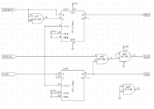
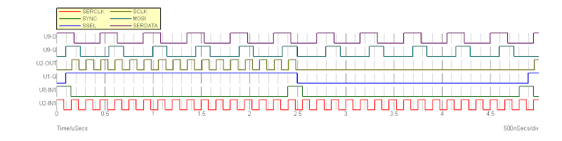
I have to read a GPS front-end output with my mbed. This is serial stream of bits running at 6.5MHz (see below)


Basically it can be considered as a 1-bit ADC with two outputs (clock and data): the clock runs at 6.5MHz and the data is 1bit wide. I have been reading a bit about mbed and so far my candidates buses are SPI (SSP) and I2S. I have some doubts about both though.. namely the SPI likes framing and the I2S is usually used at much lower speeds.

I just tried the SPISlave library so far,


SPISlave spiGpsAdc(p11, NC, p13, p14);


connecting p11 (MOSI) to the data line, p13 (SCK) to the clock, and shorting a mbed DigitalOut pin with the "chip select" of the SPISlave on p14:


DigitalOut mbedCS(p21);                // used to loopback a CS to the SPISlave


but this code


    // 
    // GET THE DATA SNAPSHOT FROM THE GPS FRONT-END
    //
    // Disable the reception of data from ADC for the moment
    mbedCS = 1;
    spiGpsAdc.format(8,1);
    //spiGpsAdc.frequency(6500000); // FIXME Should I set the clock here? mbed should be slave..    

    ptMem = (unsigned char*) malloc(16*1024);
    if (NULL != ptMem) {
        // Write in memory, probably need DMA later?
        myled2 = 1;

        k = 0;
        spiGpsAdc.reply(0x96);              // Prime SPI with first reply
        mbedCS = 0;
        while (k < (16*1024)) {
            if(spiGpsAdc.receive()) {
                ptMem[k] = spiGpsAdc.read();   // Read byte from master
                k++;
            }
        }
        mbedCS = 1;
        myled2 = 0;
    }

never exits the loop.


Could someone shed some light?


Regards,

Michele

17 Jan 2011 . Edited: 17 Jan 2011

Well,

I had a look at this library:

http://mbed.org/users/Pinski1/libraries/I2S/liy2gs

written by Robert K.

On Wikipedia I read:

In a Mono system, the word clock will pulse one bit clock length to signal the start of the next word, but will no longer be square, rather all Bit clocking transitions will occur with the word clock either high or low.

and the user manual of the LPC17xx seems to suggest that the I2S protocol in slave mode really needs a WS (Word Select) line that I don't have:

The receive channel will start receiving data after a change of WS. When word select becomes low it expects this data to be left data, when WS is high received data is expected to be right data. Reception will stop when the bit counter has reached the limit set by wordwidth. On the next change of WS the received data will be stored in the appropriate hold register. When complete data is available it will be written into the receive FIFO.

Obviously in master mode, the LPC17xx could generate the WS signal using a counter.. but the clock on the mbed is far too inaccurate to drive a GPS receiver.. even replacing it with a TCXO could not solve the problem as the reference PCLK comes from the internal PLL anyway (page 29) and nothing about its phase noise is specified - which is understandable in a MCU manual.

So I think I have two options: a complex path through I2S, or a SPI. Could anybody speculate a bit on this?

Cheers,

Mic

17 Jan 2011

From the timing diagram it appears that it's 16bits of data so why not put the SPISlave into 16bit mode?

Also, it's not clear from your post as to which clock edge DIN and SYNC are valid? The SPI modules use the LPC17xx SSP peripherals. These can be controlled via a dedicated SSEL signal. The SYNC signal appears to closely match the SSP requirements (active low). However, it all depends on the clock edge and what it's meaning.

For example, after SYNC goes low it maybe that we've missing the first bit of data. If that's the case you could feed DIN through a flip-flop clocked on the CLK line to "delay" it by one clock pulse (extra hardware I know).

Also, is this a continuous data stream or does it burst? I know GPS serial data via RS232 often bursts NMEA messages each second. It almost looks like the same thing but you're reading raw data? What device is outputting these signals? Knowing that can often help in formulating a solution.

17 Jan 2011

Hello Andy,

Thank you very much for the answer... as the LA shows, DIN and SYNC change with the rising edge of CLK.

SPI with 16bits with CPOL = 0, CPHA = 1 is the first thing I tried (using the mbed libraries) and I will go back on it later today accessing the registers directly. In fact, the manual says at page :

For continuous back-to-back transfers, the SSEL pin is held LOW between successive data words and termination is the same as that of the single word transfer

According to the MAX2769 data sheet,

A DATASYNC signal is used to signal the beginning of each valid 16-bit data slice.

and I can see from the LA that, if I use the framing signal, I shall delay it by one clock (as you say) because that positive pulse is corresponding to the first bit of the 16-bit word.

In principle though the data are coming out in a continuous stream (the MAX2769 works basically as a simple 1-bit ADC) so I should not need SYNC.

Does this answer your questions?

Thanks again,

Michele

17 Jan 2011

Quote:

as the LA shows, DIN and SYNC change with the rising edge of CLK

That suggests to me that the data on the single bit signal is valid (should be sampled) on the falling edge of the CLK signal (it must be stable for some time Tsetup prior to the clock transistion).

I've just had a look at the datasheet for the device and I must say, imho, it's a rare occasion that a Maxim datasheet leaves you "reading between the lines" as to what it means. They provide a timing diagram and setup/hold time data table for the controlling SPI interface but then only provide a few lines of text describing the DSP serial output format. No timing diagram, no setup/hold data table. Rather odd for a technical datasheet. Perhaps that ADC serial interface is designed to input to another propietry device? Anyway, like yourself, it would leave me reaching for my LA to figure it out.

Given that Farnell want £399.46 for an Eval kit I doubt I'll be connecting it to my LA !!

Refering to the LPC17xx datasheet, page 416 you can see Fig78 appears to be the "fit" to the timimg diagram. The question is, looking at your timing diagram, is the first data bit sampled on the falling clock edge while DATASYNC is high or is the first valid bit the falling edge of CLK after DATASYNC goes low? If it's the later then I would have expected one of the LPX17xx SSP ports could read this in slave mode using the setup shown in Fig78. If it's the former then you may need to delay the data signal by one clock cycle.

Hope that helps.

17 Jan 2011

Hello Andy,

I agree with you with the datasheet being rather criptic. But it's the former timing and I nuple-checked just now.

I think the problem is that mbed libraries don't like a continuous back-to-back transfer where the SSEL pin does not come back between successive data words.. that's probably why my

spiGpsAdc.receive()

never returns '1'. What a pity...

Thanks anyway for the super support.

Michele


17 Jan 2011

Actually, although I can't afford the expensive Eval kit, I can reproduce the basic timing with one Mbed and then use another Mbed to see if I can "shoe-horn" the data into an SPI slave. It's on occasions like this where I would depart from using an Mbed library and hand code using LPC17xx.h at the peripheral register level.

I'll have a play later and see if I can come up with something :)

17 Jan 2011

Hi Andy,

I really could not hope for better, but let me write some code and do the hard part... I don't want to waste too much of your time which I might hope to use later, when I am in real trouble ;)


Bests,

Michele

18 Jan 2011

Hi Michele

Well, I gave it a shot with two mbeds. One to recreate your waveforms as shown in the above timing diagram. The other to attempt to read it.

Alas, I didn't have much success. Using an SSP(SPI) in 16bit mode it just wasn't possible to read all the bits. Because bit0 occurs during the SYNC high phase, using SYNC into the SSEL input just meant it always missed bit0. Even delaying the clk and data by one bit with flip-flops just moved the problem to the other end and it missed bit15 (which was expected).

I tried a "software solution" using InterruptIn and DigitalIn. I was able to read the data but only with the CLK at a useless 500KHz, no where near the 6.5MHz needed.

So, I guess your last option is to convert the 16bit serial data into parallel data with a CPLD (funny that, Maxim make those too!).

You can find all my test code here. It's far from neat and probably would take some reading but I added comments.

regards, Andy

18 Jan 2011 . Edited: 18 Jan 2011

Michele -

What about attacking from a totally different direction?

Here is a back-of-the-envelope design for a simple two-chip test circuit that eliminates the back-to-back transfers. The idea is to discard every other sample from the GPS.

It uses one 74HCT112 negative-edge triggered J-K flip/flop, and one 74HCT00 quadruple NAND gate.

Referring to the schematic diagram below, here is a description of the operation.

Flip/flop U1B divides the SYNC signal by 2 before passing it on to the SSEL pin of the mbed. Thus, the mbed's SPI module will be selected for the interval between one SYNC pulse and the next, so it will capture the 16 bits of data that intervene. Then SSEL drops for the interval between the second SYNC pulse and the third, which effectively discards the next 16 bits of data. The cycle repeats continually. The flip/flop changes on the negative edge of SERCLK, so it captures the change in SYNC that happened on the preceding rising edge.

The SSEL signal is used to gate the SERCLK (via U2B) before passing it on to the SCLK pin of the mbed. This produces bursts of 16 clock cycles, synchronized to SSEL.

Finally, flip/flop U1A is used to delay SERDATA by one-half SERCLK cycle, before passing it along to the mbed's MOSI pin. This delay is needed to maintain the timing relationship between clock and data.

One important note -- with these changes, the active edge of the SPI clock becomes the **rising** edge. The mbed needs to be configured correspondingly, which I assume is possible (if not, try removing U2A which will un-invert SCLK).

Here is what the timing should look like (please ignore the labels to the left of the traces - they are artifacts

18 Jan 2011

user Hexley Ball wrote:

Michele -

What about attacking from a totally different direction?

Here is a back-of-the-envelope design for a simple two-chip test circuit that eliminates the back-to-back transfers. The idea is to discard every other sample from the GPS.

It uses one 74HCT112 negative-edge triggered J-K flip/flop, and one 74HCT00 quadruple NAND gate.

Referring to the schematic diagram below, here is a description of the operation.

Flip/flop U1B divides the SYNC signal by 2 before passing it on to the SSEL pin of the mbed. Thus, the mbed's SPI module will be selected for the interval between one SYNC pulse and the next, so it will capture the 16 bits of data that intervene. Then SSEL drops for the interval between the second SYNC pulse and the third, which effectively discards the next 16 bits of data. The cycle repeats continually. The flip/flop changes on the negative edge of SERCLK, so it captures the change in SYNC that happened on the preceding rising edge.

The SSEL signal is used to gate the SERCLK (via U2B) before passing it on to the SCLK pin of the mbed. This produces bursts of 16 clock cycles, synchronized to SSEL.

Finally, flip/flop U1A is used to delay SERDATA by one-half SERCLK cycle, before passing it along to the mbed's MOSI pin. This delay is needed to maintain the timing relationship between clock and data.

One important note -- with these changes, the active edge of the SPI clock becomes the **rising** edge. The mbed needs to be configured correspondingly, which I assume is possible (if not, try removing U2A which will un-invert SCLK).

Here is what the timing should look like (please ignore the labels to the left of the traces - they are artifacts of a rather quick-and-dirty simulation :-)

18 Jan 2011

I had a little bit of success by simply shortening the SYNC pule with an RC circuit. But not only is it the worst kind of "poor man's fix" it doesn't like the high speeds and is hit and miss.

I think what it boils down do is you'll need some form of external hardware. Whether it be a CPLD to convert serial to parallel or to "mop up" you own circuit as above (or just use that as is) the point is the LPC17xx on it's own isn't going to manage it.

I'm still wondering why Maxim designed teh DSP serial output like this given they went to teh trouble of actually putting in an SPI port for device control. What is the actual intended target of this serial stream?

18 Jan 2011

Hi,

Thanks a lot for all the answers. Hexley, your solution is very clever: I'm really learning something here. Problem is that LPC17xx + MAX2769 have to fit an extremely small device so I'd rather avoid having more ICs to fit the PCB. And personally, I would rather use a simple configurable logic rather than discrete logic, so Andy a CPLD would be perfect.

In my specific case though I am thinking of avoiding to use the SYNC... in this specific case in fact losing the framing information would not affect the consistency of the stream as long as I capture one bit at every rising (actually falling) edge of the serial clock. From what I read in the UM at pg416

For continuous back-to-back transfers, the SSEL pin is held LOW between successive data words and termination is the same as that of the single word transfer.

I think it should be possible to read serial data using only two wires and a "fake" SSEL.

If my LPC17xx.h code does not work, then I will have to compromise :)

Cheers,

Mic


25 Jan 2011

Hi Andy,

Would you have any idea why this code

Import programatlas

hangs on the while loop in MAX2769SSP0::Read()? It seems that the SSP0 port stays IDLE (does not receive) in slave mode with a CLK of 6.5MHz. I am trying to understand why...

Regards, Michele

25 Jan 2011

Ouch!

Following the suggestion (trick) of Gary Johnson in here if I simply do:

  pGpsAdc = new SPISlave(p11, p12, p13, p14); // data, clock, frame
  pGpsAdc->format(16,0);        
  LPC_SSP0->CR0 |= 0x0010; // switch to TI mode

  k = 0;
  while(k < N_XFER) {
    if ((LPC_SSP0->SR) & 0x4) {
      ptMem16[k++] = (uint16_t) (LPC_SSP0->DR & 0xFFFF);
    }
  }

Then it works! How is declaring an SPISlave object different from using the LPC17xx.h registers as I did?

Regards, Michele

25 Jan 2011

Michele -

SPI and TI SSI are different modes. They are documented in Chapter 18 of the LPC17xx User's Manual.

When you put the SSP0 controller in TI SSI mode, you are no longer using the mbed library to handle the data for you (since you took it out of SPI mode). Declaring the SPISlave object simply did the ugly deed of setting up the SSP0 registers for you, except for putting it in TI mode. You could set up all the registers yourself, or you could define a SSISlave class and share it with all of us. ;-)

Your next logical step is to set up a DMA to buffer the receive data for you. Be sure to add that to your SSI class, if you don't mind!

Now if I could just get my SSI receiver working...

Regards,

- Gary

25 Jan 2011

Hello Gary,

Yes I know very well that chapter of the User Manual :(

The TI protocol seems kind of suitable to my "DSP interface" timing... even if the SYNC happens at the LSB(k) rather than at the MSB(k+1), the integrity of the sequence is maintained (no bit loss). The thing is, I tried to set up the registers myself (the "ugly deed" as you say) in the class MAX2769SSP0 which I have posted. That did not have the same effect than declaring a SPISlave on SSP0 and then tweaking the CR0. I am just wondering if the SPISlave class does something more than mine, or if I simply have a bug. Unfortunately SPISlave is not open source. But I am sure you understand that before I write a SSISlave class I need to understand the issue.

On a separate note, something that still confuses me is the existence of SPISlave::frequency()... if the mbed is slave the clock comes from somewhere else so why needing to define it?

Anyway, I'll keep you posted on my progress.. and I will try to have a look at your SSI receiver if you allow me.

Regards, Michele

25 Jan 2011

Michele -

I am sorry I didn't understand your question before. I did not look at your code before I posted. Obviously you are making progress by changing the registers.

I had a lot of success by dumping the registers before and after the mbed library works on them. That way I could see what they change as they set them up. If you try it, maybe you'll find one that they set up but you forgot about.

For example, I used the following code to watch them set up SSP0 as SPI:

    printf ("SSP0 BASE = %08X\r\n", LPC_SSP0);
    printf ("SSP0: CR0  = %08X\r\n", LPC_SSP0->CR0);
    printf ("SSP0: CR1  = %08X\r\n", LPC_SSP0->CR1);
    printf ("SSP0: SR  = %08X\r\n", LPC_SSP0->SR);
    printf ("SSP0: CPSR = %08X\r\n", LPC_SSP0->CPSR);
    device.format(8, 0);          // Device 8 bit mode 0
    printf ("SSP0 BASE = %08X\r\n", LPC_SSP0);
    printf ("SSP0: CR0  = %08X\r\n", LPC_SSP0->CR0);
    printf ("SSP0: CR1  = %08X\r\n", LPC_SSP0->CR1);
    printf ("SSP0: SR  = %08X\r\n", LPC_SSP0->SR);
    printf ("SSP0: CPSR = %08X\r\n", LPC_SSP0->CPSR);
    device.frequency(2000000);    // Device bit rate
    printf ("SSP0 BASE = %08X\r\n", LPC_SSP0);
    printf ("SSP0: CR0  = %08X\r\n", LPC_SSP0->CR0);
    printf ("SSP0: CR1  = %08X\r\n", LPC_SSP0->CR1);
    printf ("SSP0: SR  = %08X\r\n", LPC_SSP0->SR);
    printf ("SSP0: CPSR = %08X\r\n", LPC_SSP0->CPSR);

I generally dump everything that seems to be involved with the device I'm playing with. It's the simplest way I can find that shows me what the mbed library is doing.

As for my SSI troubles, I have a continuous bit stream and bit clock but no frame sync. Since it's continuous, I can't use SPI, and since I have no frame sync, the SSP won't receive properly. I'm trying to create a sync pulse using timer CAP and MAT pins, but the SSP doesn't like frame sync on for four bits and then off for four more.

Regards,

- Gary

26 Jan 2011

Hi Gary,

Thank you for the insight on CAP and MAT... very interesting indeed. If you generate that kind of pattern, I bet you tried already I2S in stereo mode?

Cheers, Michele

26 Jan 2011

Michele -

I have not tried I2S yet, but I have read the User's Manual several times to see if I should try it. It seems even more cumbersome than SSP, but perhaps you have a point. If I stretch the word clock to 8 bits, maybe it would receive something.

Of course, I still have the pesky chore of word-aligning the data after I receive it, but that's a small price compared to not receiving the data at all. The data bursts are short enough that I should be able to wait until I get all of the data and then sync it up manually. The problem so far is that I don't really get any data.

I have to rewire my setup to try I2S, but I think I'll do it. Thanks for the nudge.

Regards,

- Gary

26 Jan 2011

Hi Gary,

Forgive if I ask, but what kind of chip is this one you're dealing with? How can it miss a frame signal but output a word-aligned bitstream?

Regards, Mic

26 Jan 2011

Michele -

Picture your GPS example, except that somebody decided to be mean and not give you the word sync. All I get from my device is bits and a clock. I have to sync the words after I receive them.

So far, though, that's not a problem since I can't receive the bits.

Regards,

- Gary