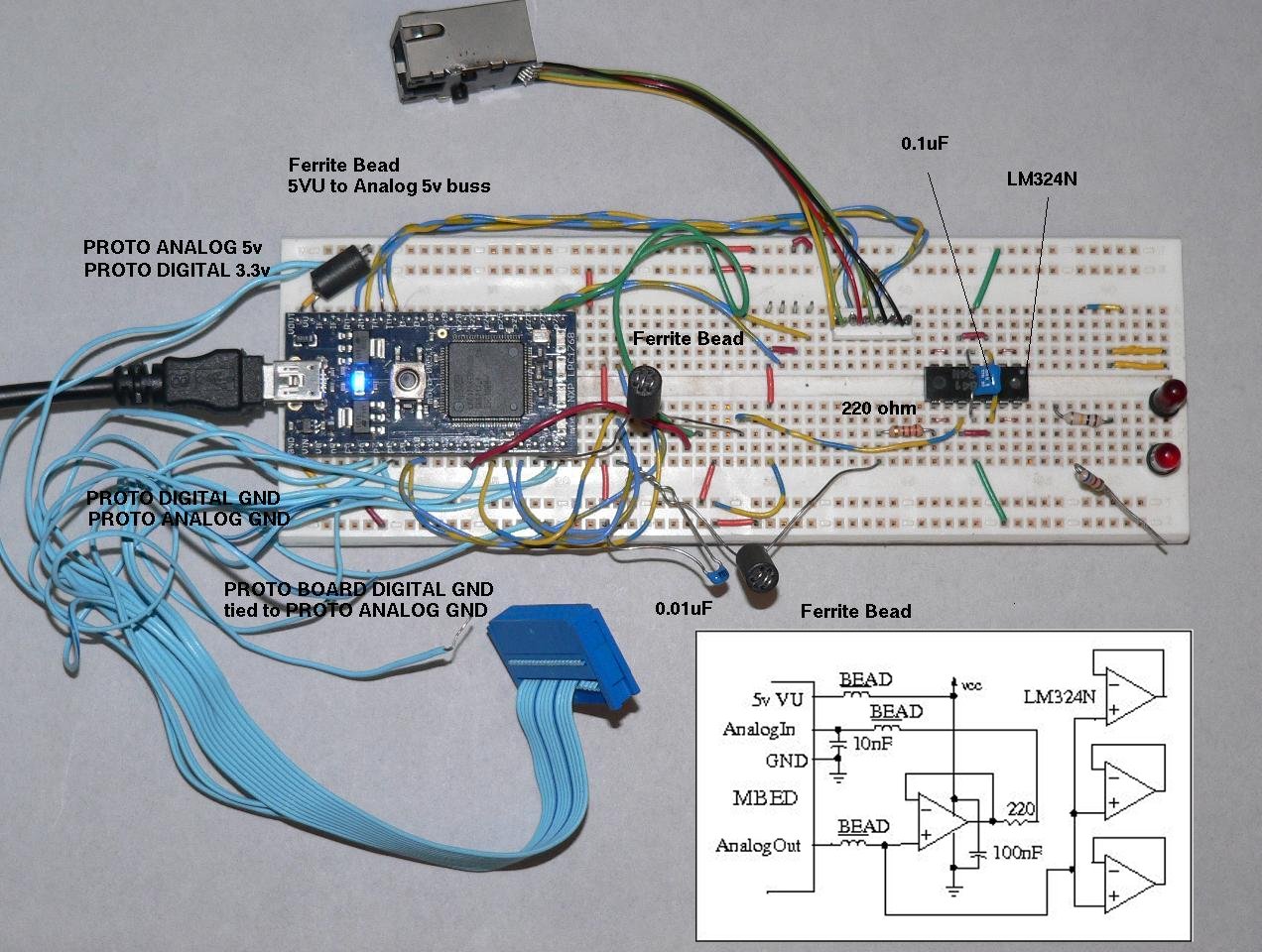
Yes, in the DAC to ADC bead test the bead was directly between the AnalogOut and a AnalogIn pin. The chosen AnalogIn pin needs the capacitor at the pin to digital ground.
In my current test I have modified the DAC to ADC test setup to include a LM324 OpAmp in the pathway. The OpAmp is configured as a non-inverting unity gain amplifier. The unused OpAmps are also configured as unity gain amplifiers. Their postive inputs should be either tied to analog ground or to a source. To maximize possible noise I connected them to the AnalogOut signal.
In the following picture you can see my prototype board is a messy layout which should be susceptible to picking up and/or emitting stray signals. The ribbon cable assembly usually goes to my LGCD4531 LCD. The RJ45 MagJack is dangling. Other currently unused leads are still connected.
The LM324 can only drive it's output to within 1.5 volts of its Vcc so to get a full 3.3 volt swing it's Vcc can be tied to a 5v source allowing the output to go to 3.5 volts. Since I am using unity gain on the OpAmp and it's input is coming from the MDED AnalogOUT then the maximum voltage expected is 3.3 volts which is fed back into a MBED AnalogIn. If you add gain, you may need to protect the MBED from overvoltage on the ADC. Remember, although the MBED digital inputs are 5v tolerant, it's analog inputs are not.
In the picture you can see that I derived my Analog 5v source from the MBED VU output on pin 39. I coupled this via a BEAD to the top power rail on the protoboard which I then use as the analog power rail. The bottom powerail is used as the analog ground and is tied back to the digital ground rail on the far left. I did not feel it necessary to couple grounds with a bead.
Since the MBED may have an inherent RF noise problem I passed the AnalogOut through a BEAD to reduce conducting that noise to the OpAmps. Notice that I have not really tried to use short leads on the BEADS or the AnalogIn Capacitor. Note the lengths of the wires extending from the MBED to where the LM324 OpAmp actually is.
Also, notice that I tied the AnalogIn capacitor from the chosen AnalogIn pin directly to digital ground. Since the noise being seen at the pin is probably coming from an internal digital pathway that noise needs to be returnd to the digital ground. Connecting the capacitor to analog ground will just pass that noise into the analog ground loop where it can be conducted to the amplifiers. There is a definite noticable difference which ground that capcitor is attached to.
The results I got was virtually noise free. I have forwarded the dump file to Misha for analysis.

Hi Guys,
I agree that no opamps are better. But for my purpose I want to amplify a part of the signal and give it an offset for better accuracy. The signal differences I want to measure are 10ths of uV.
Schematics tested and working for my purpose:
The circuit in my previous posts was only to determine the source of the conversion errors, it looks like grounding and emmissions caused by the bread board are causing them.
About the clock frequency I mentioned in my earlier post, I made a mistake in giving the scope settings for the image. Here is a new shot, the settings are horizontal 0.05 uSec/div and vertically 2 mV/div:
So the signal frequency is roughly 1.6 * 0.05 uSec = 0.08 uSec, which translate in roughly 12 MHz. This signal occurred on pin 20 (analog in channel 0) of the mbed.