SPI Investigation / FeRAM
The Problem
I am working on using the mbed for some image processing stuff for my MSc project and I soon found that the mbed 'runs out' of memory around 22k. I am using images in RAW format that are 160*120 pixels in 16-bit colour, meaning the arrays they are stored in are 160*120*2 = 38400 bytes in size. Too big to store onboard. So I have to look at external memory. The choices I have are basically thus:
- Use a flash memory chip like the AT45 Family of ICs
- Use a SPI EEPROM IC like the 23k256 IC from Microchip
- Use some parallel SRAM IC
- Use some other type of flash memory - like SD Card, USB drive, LocalFileSystem, etc...
I want to write data to and from external memory like 'bat outta hell quick' meaning the system has as much time as possible to do the image processing. But I also need the ability to manipulate single bytes of data.
Early Testing
I wrote a page here that tests out the read / write times of some of these devices, and I have tested a few others that I have not documented (shame on me!)and I can rule out a few thing right off the bat.
- All the flash chips that I have found will be too slow. This is because they all operate in blocks of usually 512 bytes, and you have to read and write a whole block at a time. This means that to read the value of a single pixel in my image, I will have to read in 511 pixels that I'm not too interested in. Sure I could buffer them and try to do something clever but I think I'm going to rule this out straight away.
- For pretty much the same reason - which is supported by my testing, I'm ruling out USB sticks and SD Cards that use the SD Card file system.
- Also on the strength of the testing the LocalFileSystem is out of the window as well. I must admit that this is the 'best' solution from the point of view that it requires no external components. But it's too slow for what I want.
So this leaves SPI memory and parallel memory.
Parallel SRAM
This should be the fastest, and it is the closest to what you might find in a PC. Looking at a datasheet for a typical IC and I see lots of timing info in the 10's of nanoseconds. But the more I look into this I see 2 big problems.
- I'm looking at chips that have >1Mb (1 mega bit - all of these type of ICs state their capacities in bits) meaning that I will need around 17 address lines. On top of this I will need a chip select line and maybe something else. Assuming that I can use the same lines for address and data lines, lets say I need 20 lines of IO. That is a lot!
- It's all well and good knowing the IC has an access time of 60ns, but how fast can the mbed actually toggle its pins to get the data in and out?
This is enough to put me off using parallel SRAM so I will look at SPI.
SPI FeRAM
I found some FeRAM and am keen to have a play with it. FeRAM promises to be quicker than EEPROM. The IC is the FM25H20-DG from Ramtron and can be found at Farnell here. The highest SPI frequency supported by the chip is 40MHz and the specs say that the chip can be written to at a whopping 5 MB/s (that is bytes this time!)
So can the mbed write data out at that rate? Lets look at the SPI port writing with a scope. Using the simple SPI program below I can probe the SPI CLK line (p7)
#include "mbed.h"

SPI my_spi(p5, p6, p7);

int main() {
    while(1) {
        my_spi.write(0);
    }
}
And the output on the scope...
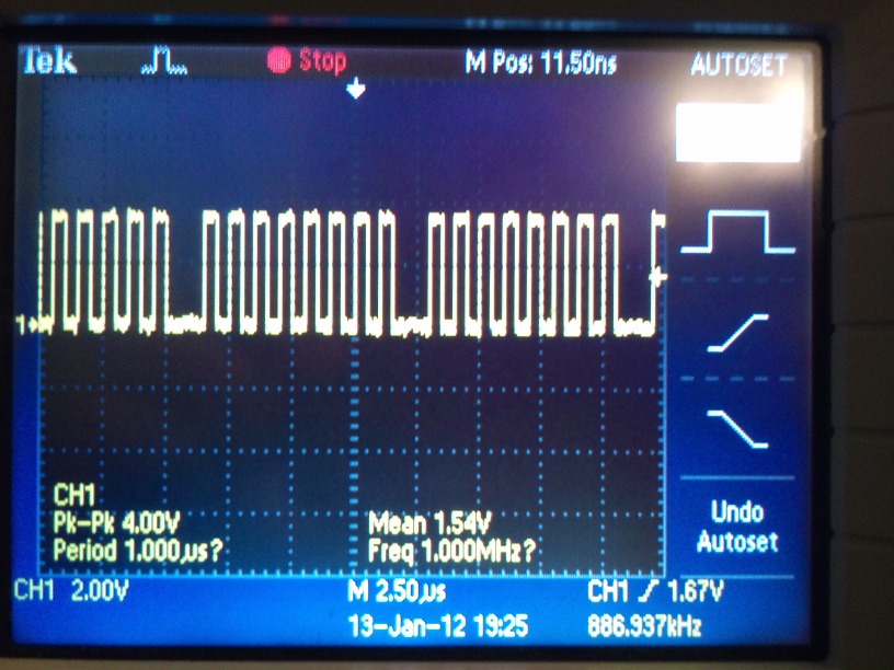
This picture shows the SPI CLK line and a small delay (1.56 us) can be seen between the last clock of one byte and the first clock of the next byte.
I then changed the SPI frequency to 32MHz (the closest I can get to 40MHz), and the delay is still around 1.2 us. Still 1.2 - 1.56us, not such a big deal? is it?
Why this IS a big deal
Well to write a byte in a location with this IC I need to write 5 bytes of data to the chip. So the delay will be 8us for the full write. For 38400 bytes (1 full image) this will become 300 ms! 0.3 seconds just sitting round waiting for the SPI to sort itself out.
This post on the forum seems to suggest that if we change the SPI format to mode 3 then this delay will disappear. So lets try it...
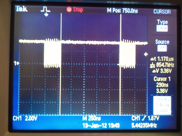
This shows the SPI CLK pin going up and down like the clappers (at 32MHz) with the delay still alive and well. Notice how the clock is normally high now instead of normally low, and the proportion of the time that the SPI clock is idle.
What can I do about it?
Well, as suggested by Nenad Milosevic in the above post I am accessing the SPI interface directly to speed things up. To start with I try out the code below...
#include "mbed.h"

SPI my_spi(p5, p6, p7);

int main() {
    my_spi.frequency(32000000);
    while (1) {
        while (!(LPC_SSP1->SR & 2))   // If TNF-Bit = 0 (FIFO full) then wait
            ;
        LPC_SSP1->DR = 0x00;          // Write to FIFO data register
    }
}
This code pimps up the SPI frequency the goes into an endless loop that waits until the SPI is free to be written to. When its free it writes the data to the SPI. This should make the SPI port run as fast as possible. The result...
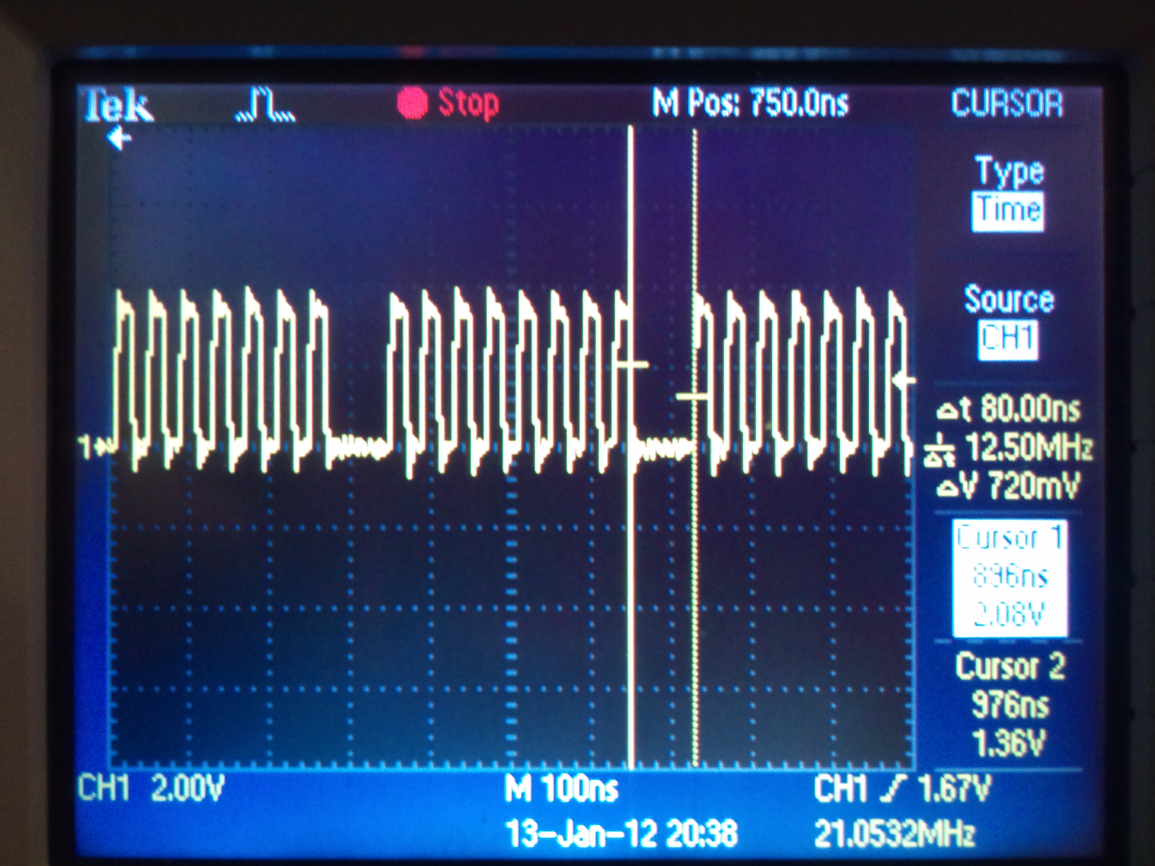
This shows that using this code the SPI port can be written to with only a 80ns delay between bytes. This will take the 0.3 second delay for transferring an image down to around 15ms.
Benchmarking the current API
I really should check before using this code I can write and read to the FeRAM!
So I'll write some code using the normal SPI API first that will write a value to the FeRAM and then read it back. This will prove that the FeRAM is wired up correctly and set a benchmark that I can try to improve on using my custom code.
The code I used to benchmark the system is shown below.
#include "mbed.h"

SPI my_spi(p5, p6, p7);
DigitalOut cs(p8);
Serial pc(USBTX,USBRX);

int main() {
    // Increase the SPI frequency from the default 1Mhz
    my_spi.frequency(32000000); // 32MHz is the fastest mbed frequency supported by the FeRAM

    // To start with I need the chip select high and wait 1ms after powering up
    cs = 1;                     // Bring chip select high to start with
    wait(0.001);                // Must wait 1ms after power on before using FeRAM

    // According to the FeRAM datasheet first I need to write enable the FeRAM
    cs = 0;                     // Bring chip select low to write to FeRAM
    my_spi.write(0x06);         // Send WREN command
    cs = 1;                     // Bring chip select high to stop writing

    // Thought I would wait a bit to get a cleaner scope trace
    wait_us(10);

/**** START OF WRITE SEQUENCE ****/
    cs = 0;                     // Bring chip select low to write to FeRAM
    my_spi.write(0x02);         // Send write command
    my_spi.write(0x00);         // Send top address byte to wrtie to
    my_spi.write(0xFF);         // Send Middle address byte to wrtie to
    my_spi.write(0xFF);         // Send Bottom address byte to wrtie to
    my_spi.write(0x55);         // Send data to be write
    cs = 1;
/**** END OF WRITE SEQUENCE ****/

    // Thought I would wait a bit again
    wait_us(10);

/**** START OF READ SEQUENCE ****/
    int my_val;                 // Variable to store the read data
    cs = 0;
    my_spi.write(0x03);         // Send read command
    my_spi.write(0x00);         // Send top address byte to read from
    my_spi.write(0xFF);         // Send middle address byte to read from
    my_spi.write(0xFF);         // Send bottom address byte to read from
    my_val = my_spi.write(0x00);// Write dummy byte to get data
    cs = 1;
/**** END OF READ SEQUENCE ****/

    // Print the data read on screen
    pc.printf(" Value = 0x%X",my_val);
}
When run the result in TeraTerm does indeed show that the data has been written to and read successfully from the FeRAM.
When interrogated with the scope, the time it took to write to the FeRAM (the time from the falling egde of cs to the next rising edge of cs) is 7.24us. The read time was also measured at 7.24us. The scope trace for the read can be seen in the photo below.
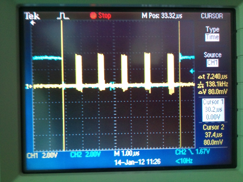
So now I have my benchmark how can I speed things up?
Wind it up son
Well as a starting point I will look at implementing my earlier custom code. I downloaded the LCP1768 user manual and studied the SSP section. I will start with the writing side of things and then move onto the reading later on.
To do everything as quick as possible I need to bring cs low and then check the transmit FIFO buffer. If there is space in the buffer I will start writing to it. I will basically do this as quick as I can for all 5 bytes. Then I need to make sure that all the data is written from the buffer before bringing cs high again to end the write sequence.
The SSPn Status Register (SSP0->SR) has bits in it that will allow me to check the status of the FIFO buffers. I'm using SSP0 only throughout this experiment. I will also write to a different memory location so as not to read back my know good data! So my first stab at some code is...
/*** My method to write to FeRAM ***/
void spi_write (unsigned char data) {
    // First don't write to the FIFO buffer if it is full
    while (!(LPC_SSP1->SR & TNF))   // While TNF-Bit = 0 (FIFO full)...
        ;                           // Wait
    LPC_SSP1->DR = data;            // Write to FIFO buffer
}
For the method to write to SPI, and...
/**** START OF WRITE SEQUENCE ****/
    cs = 0;                         // Bring chip select low to write to FeRAM
    spi_write(0x02);                // Send write command
    spi_write(0x00);                // Send top address byte to wrtie to
    spi_write(0x0F);                // Send Middle address byte to wrtie to
    spi_write(0xFF);                // Send Bottom address byte to wrtie to
    spi_write(0xAA);                // Send data to be write
    // Now I need to check that the FIFO transmit buffer is empty before the cs rising egde
    while (!(LPC_SSP1->SR & TNE))   // While TNE-Bit = 0 (FIFO not empty)...
        ;                           // Wait
    cs = 1;                         // Bring chip select high to stop writing
    /**** END OF WRITE SEQUENCE ****/
My new code showing the modifications to the write sequence.
And the result - it didn't work... Well I'm disappointed. So I have a little look at the scope again and see what has happened. Well the write time now is an impressive 2.03us, but the big thing I notice is that the cs is going high again before the SPI port has finished writing. After a bit of a think I realise that even though the FIFO buffer is empty (the TNE bit is set) it doesn't mean that it has completed the write out of the port. So I need a small delay in there to give the port a while to finished writing. I look again at the scope and I only need about 150ns. I don't really want to put a whole wait_us(1) command in and waste 850ns.
The mbed has a clock that runs at 96MHz - hence each clock cycle is just over 10ns. So I want to waste around 15 clock cycles. To do this I use the _ _nop(); command to waste 1 clock cycle. I could also increment a variable a few times or something but as I'm in such early stages of development I'm happy just to use this and have slightly longer code.
I try it again... And still nothing!?! I scope the output from the FeRAM and I can see the data coming out as it should... Maybe I have messed up the SPI API on that port?
Well after a bit of head scratching I figure it out. I have been merrily filling up the FIFO receive buffer and not read it before now. So all those received bytes are stacking up (and overflowing!) in the buffer. When I read one it is the one from way back, not the one I want.
I had better clean this up in the read sequence...
Speed reading
The sequence for reading will be something like this...
Bring the cs low to start the read. Then using the same method as before send out the read command (0x03) and the 3 address bytes. Now the final byte is the actual data I want to read. Before I read this I need to empty the FIFO receive buffer. This will ensure that when I read the next byte it will be the actual data I want and not one of the previous buffered bytes.
I can check when the buffer is empty so the code should be something like this...
    /**** START OF READ SEQUENCE ****/
    int my_val;                     // Variable to store the read data
    cs = 0;                         // Bring chip select low to write to FeRAM
    spi_write(0x03);                // Send read command
    spi_write(0x00);                // Send top address byte to read from
    spi_write(0x0F);                // Send middle address byte to read from
    spi_write(0xFF);                // Send bottom address byte to read from
    // Now I need to empty the FIFO receive buffer...
    while (LPC_SSP1->SR & RNE)      // While RNE-Bit = 1 (FIFO receive buffer not empty)...
        my_val = LPC_SSP1->DR;      // Read the byte in the buffer
    // Now the buffer is empty send out a dummy byte and read the buffer
    spi_write(0x00);                // Send the dummy byte
    // Wait for the byte to be received...
    while (!(LPC_SSP1->SR & RNE))   // While RNE-Bit = 0 (FIFO receive buffer empty)...
       ;                            // Wait
    my_val = LPC_SSP1->DR;          // Read the byte - this is the one we want
    cs = 1;                         // Bring chip select high to stop writing
    /**** END OF READ SEQUENCE ****/
And now TeraTerm tells me that the value stored at address is 0xAA, correct! Looking at the read sequence on the scope I get...
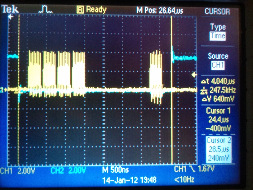
This shows the read sequence taking 4.04us, which is longer than the write. This is to be expected as it takes time to clear the FIFO receive buffer (the scope shows this takes around 1.7us).
What else can I do?
So as it stands I have reduce the write time from 7.24us to 2.20us and reduce the read time from 7.24us to 4.04us.Can I get it any faster? Well I think a little faster. Back in the forum post I mentioned earlier it showed that the format the SPI was in made a difference to the performance. Currently I am in mode 1, mode 3 is quicker. So lets see what that does to the write time...
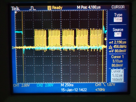
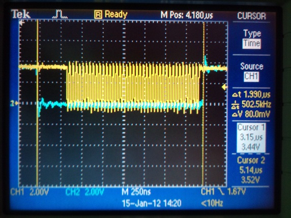
The picture on the left shows the write sequence in mode 0 (notice the gaps between each byte), and the right image shows the sequence in SPI mode 3 (no gaps). The result? The write sequence happens around 200ns faster now taking 1.99us
Anything else I can do?
Well yes, a few little things. The reason for the gaps between bytes in mode 0 are to allow the SSEL1 (slave select 1) line on the SPI port to toggle high and low again which signals the end of a byte. Mode 3 allows for continuous back-to-back transmissions where the SSEL line remains low between bytes.
Well looking at it the SSEL line does exactly what I'm using the chip select line to do. So why don't I use the SSEL? Will the standard SPI API doesn't use it, but I can configure it manually as it still comes out to pin 8. Configuring P0[6] (which is pin 8) to be SSEL is done by writing to the PINSEL0 register. If I make bit 13 high and bit 12 low in this register then it should work. The follow code should do the trick. This will also allow me to get rid of the ugly _ _nop() functions that I called earlier to produce a 150ns delay as the SSEL line should do it for me.
// Set up SSEL1
LPC_PINCON->PINSEL0 |= 0x00002000;
So I'll test it and see what happens...
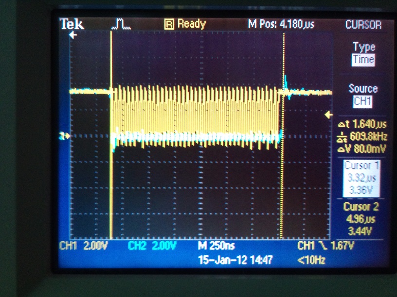
As you can see form the photo above the write time is now down to 1.64us.
So all is good?
Well no, I also find out that due to the gap in the read sequence that clears the FIFO buffer the SSEL line goes high before the last byte is written and messes up the read. But I can get around this I think.
No matter how full the FIFO receive buffer is the byte I want (the read data) will always be the last one in the buffer. So I can happily read in values (even let the buffer overflow) and then when all is done just read the buffer until it is empty - the last value I have will be the one I want. So a quick change to the code is due...
The final program is shown here...
More testing
I have done some testing and found that the WREN command needs to be sent EVERY time that the FeRAM is written to. Furthermore the SSEL line MUST go high between the WREN command and the WRITE command.
I make a few changes to the method to reflect this and test some more. Finally I end up with this program...
Conclusion
I have tested the speed of writing and reading to and from the FeRAM and with these code changes I have reduced the time it takes to write a byte to FeRAM from 7.24us to 2.11us and cut the read time from 7.24us to around 2.63us.
I now need to test for reading and writing multiple bytes and bring this all together in a library. Writing mulitple bytes will speed up the system further as I will not have the overhead of writing the WREN or WRITE commands or the address each time.
After a bit more work the library has been constructed and is posted below...
Import libraryFeRAM
A library for using FeRAM from Ramtron
I have done some work on it so that it will work with either of the SPI ports - just declare mosi, miso, and sclk the same way as normal and wire up chip select to p8 or p14 (you don't need to declare this pin the code however)
Testing shows it is around 2.5X as quick as the standard SPI API so I'm quite happy.
The hello world program can be found here...
Import programFeRAM_Hello_World
A simple hello world program that writes and reads to and from FeRAM
4 comments on SPI Investigation / FeRAM:
Please log in to post comments.

You probably dont want to use as many as 17 of the precious mbed pins as addresslines. That means you need to use an external serial portexpander (like the MCP23S17 for SPI) to provide address and even datalines to the parallel SRAM. This means a single bytewrite will probably be as slow/fast as writing to a regular SPI memory since you have to shift out all addressbits in serial. However, it gets worse when you write blocks of data since the SPI memory has the address auto-increment features which you dont have on your SRAM.
Some additional hardware like a counter that provides your SRAM addresslines may help: use one mbed pin to provide a pulse that increments a presettable addresscounter. Now you only need to provide the data for each write. You may be able to combine the incr-address pin with the writepin for the SRAM.
I think I would recommend to stick with the fastest possible SPI RAM. You may however be able to use the DMA features of mbed to send this data to the RAM. That allows mbed to do other useful stuff in parallel since the DMA does not require the CPU.