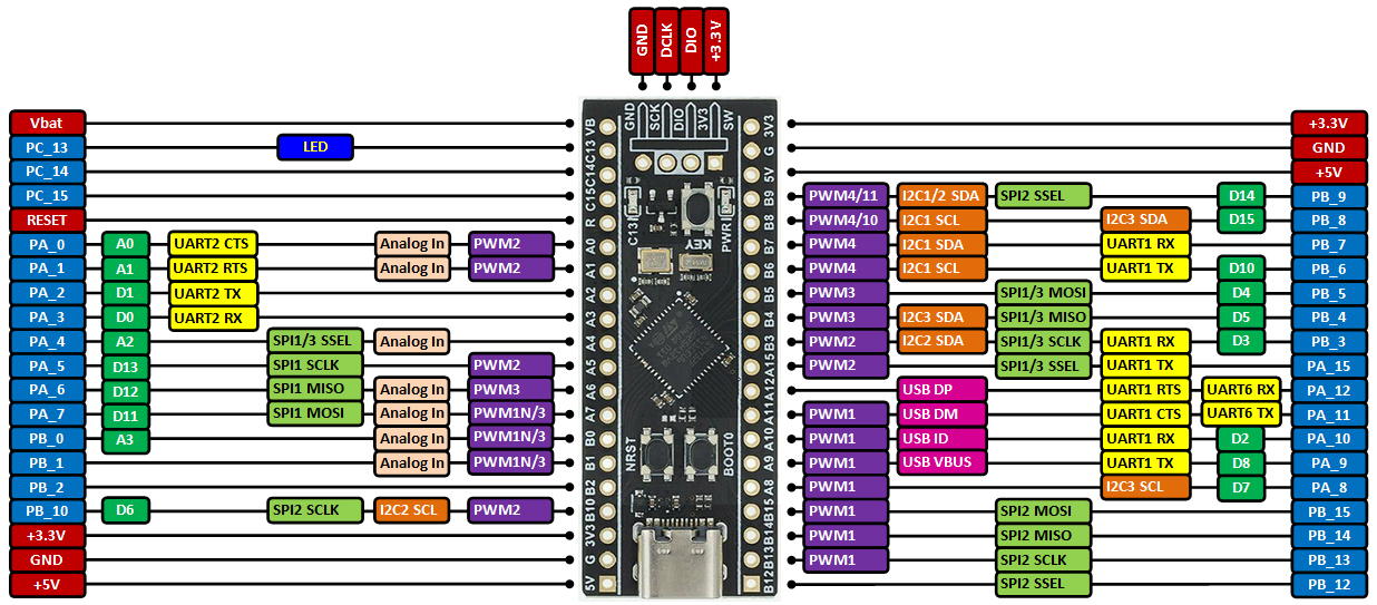
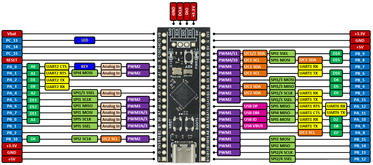
BLACKPILL custom target.
BLACKPILL custom target
Board pinout
When equipped with STM32F401CCU6:
When equipped with STM32F411CEU6:
Advantages of the BLACKPILL custom target over the NUCLEO_F401RE/ NUCLEO_F411RE
- The onboard external 25 MHz crystal is used as system clock source rather than the less precise internal 16 MHz RC oscillator.
- The onboard LED works as LED1 in programs.
- The onboard KEY on STM32F411CEU6 boards works as USER_BUTTON pin in programs.
- You can use the USB peripheral in your programs and connect the board to the PC over the onboard USB connector. An example of using the USB peripheral as USBSerial (12 Mbit/s) is available here.
Building programs for the BLACKPILL custom target in Mbed Studio
- Connect an STM32 ST-Link programmer to your BLACKPILL board and PC (see below for more details).
- Create a new program in the Mbed Studio IDE.
- Right-click on the program's root folder and in the popup window select
Add library...
- Copy&paste the text https://os.mbed.com/users/hudakz/code/BLACKPILL_Custom_Target into the
Git or os.mbed.com URLedit box and click on theNextbutton.
- Open the drop-list and select
defaultasBranch or tagand click on theFinishbutton.
- Open the
BLACKPILL_Custom_Targetfolder and according to you board drag&drop theTARGET_BLACKPILL_F401CCor theTARGET_BLACKPILL_F411CEfolder and thecustom_targets.jsonfile one by one to the root folder of your program.
- Delete the
BLACKPILL_Custom_Targetfolder from your project. (Right-click and select delete).
- Open the
Targetdrop-list and click on the button with a "chip" icon on it (Manage custom targets) .
- Open the
USB devicedrop-list and select your STM32 ST-Link programmer.
- Open the
Build targetdrop-list and according to your board selectBLACKPILL_F401CCorBLACKPILL_F411CE.
- Click on the
Save Allbutton.
- Build your program (click on hammer button).
For more info visit
Import programBlackpill_Hello
Using low cost Blackpill (STM32F411CEU6) boards with mbed.
Diff: TARGET_BLACKPILL_F411CE/system_clock.c
- Revision:
- 7:3a74f7149fa4
diff -r e6fa20f2675a -r 3a74f7149fa4 TARGET_BLACKPILL_F411CE/system_clock.c
--- /dev/null	Thu Jan 01 00:00:00 1970 +0000
+++ b/TARGET_BLACKPILL_F411CE/system_clock.c	Sat Mar 19 10:08:40 2022 +0000
@@ -0,0 +1,201 @@
+/* mbed Microcontroller Library
+ * SPDX-License-Identifier: BSD-3-Clause
+ ******************************************************************************
+ *
+ * Copyright (c) 2015-2021 STMicroelectronics.
+ * All rights reserved.
+ *
+ * This software component is licensed by ST under BSD 3-Clause license,
+ * the "License"; You may not use this file except in compliance with the
+ * License. You may obtain a copy of the License at:
+ *                        opensource.org/licenses/BSD-3-Clause
+ *
+ ******************************************************************************
+ */
+
+/**
+  * This file configures the system clock as follows:
+  *----------------------------------------------------------------------
+  * System clock source | 1- USE_PLL_HSE_XTAL      | 2- USE_PLL_HSI
+  *                         (external 25 MHz xtal) |    (internal 16 MHz)
+  *----------------------------------------------------------------------
+  * USB enabled         |  NO | YES                |  NO | YES
+  *----------------------------------------------------------------------
+  * SYSCLK(MHz)         | 100 | 96                 | 100 | 96
+  * AHBCLK (MHz)        | 100 | 96                 | 100 | 96
+  * APB1CLK (MHz)       |  50 | 48                 |  50 | 48
+  * APB2CLK (MHz)       | 100 | 96                 | 100 | 96
+  *----------------------------------------------------------------------
+**/
+
+#include "stm32f4xx.h"
+#include "mbed_error.h"
+
+// clock source is selected with CLOCK_SOURCE in json config
+#define USE_PLL_HSE_EXTC     0x8  // Use external clock (ST Link MCO)
+#define USE_PLL_HSE_XTAL     0x4  // Use external xtal (X3 on board - not provided by default)
+#define USE_PLL_HSI          0x2  // Use HSI internal clock
+
+#if ( ((CLOCK_SOURCE) & USE_PLL_HSE_XTAL) || ((CLOCK_SOURCE) & USE_PLL_HSE_EXTC) )
+uint8_t SetSysClock_PLL_HSE(uint8_t bypass);
+#endif /* ((CLOCK_SOURCE) & USE_PLL_HSE_XTAL) || ((CLOCK_SOURCE) & USE_PLL_HSE_EXTC) */
+
+#if ((CLOCK_SOURCE) & USE_PLL_HSI)
+uint8_t SetSysClock_PLL_HSI(void);
+#endif /* ((CLOCK_SOURCE) & USE_PLL_HSI) */
+
+
+/**
+* @brief  Configures the System clock source, PLL Multiplier and Divider factors,
+*               AHB/APBx prescalers and Flash settings
+* @note   This function should be called only once the RCC clock configuration
+*         is reset to the default reset state (done in SystemInit() function).
+    * @param  None
+    * @retval None
+    */
+
+MBED_WEAK void SetSysClock(void)
+{
+#if ((CLOCK_SOURCE) & USE_PLL_HSE_EXTC)
+    /* 1- Try to start with HSE and external clock */
+    if (SetSysClock_PLL_HSE(1) == 0)
+#endif
+    {
+#if ((CLOCK_SOURCE) & USE_PLL_HSE_XTAL)
+        /* 2- If fail try to start with HSE and external xtal */
+        if (SetSysClock_PLL_HSE(0) == 0)
+#endif
+        {
+#if ((CLOCK_SOURCE) & USE_PLL_HSI)
+            /* 3- If fail start with HSI clock */
+            if (SetSysClock_PLL_HSI() == 0)
+#endif
+            {
+                {
+                    error("SetSysClock failed\n");
+                }
+            }
+        }
+    }
+
+    /* Output clock on MCO2 pin(PC9) for debugging purpose */
+    //HAL_RCC_MCOConfig(RCC_MCO2, RCC_MCO2SOURCE_SYSCLK, RCC_MCODIV_4);
+}
+
+#if ( ((CLOCK_SOURCE) & USE_PLL_HSE_XTAL) || ((CLOCK_SOURCE) & USE_PLL_HSE_EXTC) )
+/******************************************************************************/
+/*            PLL (clocked by HSE) used as System clock source                */
+/******************************************************************************/
+MBED_WEAK uint8_t SetSysClock_PLL_HSE(uint8_t bypass)
+{
+    RCC_OscInitTypeDef RCC_OscInitStruct;
+    RCC_ClkInitTypeDef RCC_ClkInitStruct;
+
+    /* The voltage scaling allows optimizing the power consumption when the device is
+       clocked below the maximum system frequency, to update the voltage scaling value
+       regarding system frequency refer to product datasheet. */
+    __HAL_RCC_PWR_CLK_ENABLE();
+    __HAL_PWR_VOLTAGESCALING_CONFIG(PWR_REGULATOR_VOLTAGE_SCALE2);
+
+    /* Get the Clocks configuration according to the internal RCC registers */
+    HAL_RCC_GetOscConfig(&RCC_OscInitStruct);
+
+    /* PLL could be already configured by bootlader */
+    if (RCC_OscInitStruct.PLL.PLLState != RCC_PLL_ON) {
+
+        // Enable HSE oscillator and activate PLL with HSE as source
+        RCC_OscInitStruct.OscillatorType      = RCC_OSCILLATORTYPE_HSE;
+        if (bypass == 0) {
+            RCC_OscInitStruct.HSEState          = RCC_HSE_ON;       // External 25 MHz xtal on OSC_IN/OSC_OUT
+        } else {
+            RCC_OscInitStruct.HSEState          = RCC_HSE_BYPASS;   // External 25 MHz clock on OSC_IN
+        }
+
+        RCC_OscInitStruct.PLL.PLLState = RCC_PLL_ON;
+        RCC_OscInitStruct.PLL.PLLSource = RCC_PLLSOURCE_HSE;
+        #if (CLOCK_SOURCE_USB)
+            RCC_OscInitStruct.PLL.PLLM          = 25;           // VCO input clock = 1 MHz (25 MHz / 25)
+            RCC_OscInitStruct.PLL.PLLN          = 192;          // VCO output clock = 192 MHz (1 MHz * 192)
+            RCC_OscInitStruct.PLL.PLLP          = RCC_PLLP_DIV2;// PLLCLK = 96 MHz (192 / 2)
+            RCC_OscInitStruct.PLL.PLLQ          = 4;            // USB clock = 48 MHz (192 / 4, CLOCK_SOURCE_USB = 1)
+        #else
+            RCC_OscInitStruct.PLL.PLLM          = 12;           // VCO input clock = 2.0833 MHz (25 MHz / 12)
+            RCC_OscInitStruct.PLL.PLLN          = 96;           // VCO output clock = 200 MHz (2.0833 MHz * 96)
+            RCC_OscInitStruct.PLL.PLLP          = RCC_PLLP_DIV2;// PLLCLK = 100 MHz (200 / 2)
+            RCC_OscInitStruct.PLL.PLLQ          = 4;            // USB clock = 50 MHz (200 / 4 -> USB not available)
+        #endif
+        if (HAL_RCC_OscConfig(&RCC_OscInitStruct) != HAL_OK) {
+            return 0; // FAIL
+        }
+    }
+
+    // Select PLL as system clock source and configure the HCLK, PCLK1 and PCLK2 clocks dividers
+    RCC_ClkInitStruct.ClockType = RCC_CLOCKTYPE_SYSCLK | RCC_CLOCKTYPE_HCLK | RCC_CLOCKTYPE_PCLK1 | RCC_CLOCKTYPE_PCLK2;
+    RCC_ClkInitStruct.SYSCLKSource   = RCC_SYSCLKSOURCE_PLLCLK; // 100/96 MHz
+    RCC_ClkInitStruct.AHBCLKDivider  = RCC_SYSCLK_DIV1;         // 100/96 MHz
+    RCC_ClkInitStruct.APB1CLKDivider = RCC_HCLK_DIV2;           // 50/48 MHz
+    RCC_ClkInitStruct.APB2CLKDivider = RCC_HCLK_DIV1;           // 100/96 MHz
+    if (HAL_RCC_ClockConfig(&RCC_ClkInitStruct, FLASH_LATENCY_3) != HAL_OK) {
+        return 0; // FAIL
+    }
+
+    /* Output clock on MCO1 pin(PA8) for debugging purpose */
+    //if (bypass == 0)
+    //  HAL_RCC_MCOConfig(RCC_MCO1, RCC_MCO1SOURCE_HSE, RCC_MCODIV_2); // 4 MHz with xtal
+    //else
+    //  HAL_RCC_MCOConfig(RCC_MCO1, RCC_MCO1SOURCE_HSE, RCC_MCODIV_1); // 8 MHz with external clock
+
+    return 1; // OK
+}
+#endif /* ((CLOCK_SOURCE) & USE_PLL_HSE_XTAL) || ((CLOCK_SOURCE) & USE_PLL_HSE_EXTC) */
+
+#if ((CLOCK_SOURCE) & USE_PLL_HSI)
+/******************************************************************************/
+/*            PLL (clocked by HSI) used as System clock source                */
+/******************************************************************************/
+uint8_t SetSysClock_PLL_HSI(void)
+{
+    RCC_OscInitTypeDef RCC_OscInitStruct;
+    RCC_ClkInitTypeDef RCC_ClkInitStruct;
+
+    /* The voltage scaling allows optimizing the power consumption when the device is
+       clocked below the maximum system frequency, to update the voltage scaling value
+       regarding system frequency refer to product datasheet. */
+    __HAL_RCC_PWR_CLK_ENABLE();
+    __HAL_PWR_VOLTAGESCALING_CONFIG(PWR_REGULATOR_VOLTAGE_SCALE2);
+
+    // Enable HSI oscillator and activate PLL with HSI as source
+    RCC_OscInitStruct.OscillatorType      = RCC_OSCILLATORTYPE_HSI | RCC_OSCILLATORTYPE_HSE;
+    RCC_OscInitStruct.HSIState            = RCC_HSI_ON;
+    RCC_OscInitStruct.HSEState            = RCC_HSE_OFF;
+    RCC_OscInitStruct.HSICalibrationValue = RCC_HSICALIBRATION_DEFAULT;
+    RCC_OscInitStruct.PLL.PLLState        = RCC_PLL_ON;
+    RCC_OscInitStruct.PLL.PLLSource       = RCC_PLLSOURCE_HSI;
+    RCC_OscInitStruct.PLL.PLLM            = 8;             // VCO input clock = 2 MHz (16 MHz / 8)
+#if (DEVICE_USBDEVICE)
+    RCC_OscInitStruct.PLL.PLLN            = 192;           // VCO output clock = 384 MHz (2 MHz * 192)
+#else /* DEVICE_USBDEVICE */
+    RCC_OscInitStruct.PLL.PLLN            = 200;           // VCO output clock = 400 MHz (2 MHz * 200)
+#endif /* DEVICE_USBDEVICE */
+    RCC_OscInitStruct.PLL.PLLP            = RCC_PLLP_DIV4; // PLLCLK = 100 MHz or 96 MHz (depending on DEVICE_USBDEVICE)
+    RCC_OscInitStruct.PLL.PLLQ            = 8;             // USB clock = 48 MHz (DEVICE_USBDEVICE=1)
+    if (HAL_RCC_OscConfig(&RCC_OscInitStruct) != HAL_OK) {
+        return 0; // FAIL
+    }
+
+    /* Select PLL as system clock source and configure the HCLK, PCLK1 and PCLK2 clocks dividers */
+    RCC_ClkInitStruct.ClockType      = (RCC_CLOCKTYPE_SYSCLK | RCC_CLOCKTYPE_HCLK | RCC_CLOCKTYPE_PCLK1 | RCC_CLOCKTYPE_PCLK2);
+    RCC_ClkInitStruct.SYSCLKSource = RCC_SYSCLKSOURCE_PLLCLK;
+    RCC_ClkInitStruct.AHBCLKDivider = RCC_SYSCLK_DIV1;
+    RCC_ClkInitStruct.APB1CLKDivider = RCC_HCLK_DIV2;
+    RCC_ClkInitStruct.APB2CLKDivider = RCC_HCLK_DIV1;
+    if (HAL_RCC_ClockConfig(&RCC_ClkInitStruct, FLASH_LATENCY_3) != HAL_OK) {
+        return 0; // FAIL
+    }
+
+    /* Output clock on MCO1 pin(PA8) for debugging purpose */
+    //HAL_RCC_MCOConfig(RCC_MCO1, RCC_MCO1SOURCE_HSI, RCC_MCODIV_1); // 16 MHz
+
+    return 1; // OK
+}
+#endif /* ((CLOCK_SOURCE) & USE_PLL_HSI) */


