LPC812 MAX Experiment: SPI
Experiment: Work with a Serial Bus - SPI
In this experiment you will learn how to work with the Serial Peripheral Interface Bus, or SPI bus for short. It is a synchronous bus meaning that there is an explicit clock signal. SPI builds on the master/slave concept where one unit is a master and controls the communication. The other end is the slave. Four signals are needed for communication in both directions:
- SCLK: serial clock, driven from the master
- MOSI: data signal, Master Output, Slave Input, driven from the master
- MISO: data signal, Master Input, Slave Output, driven from the slave
- SSEL or SS: Slave Select, driven from the master
Many slaves can co-exist if there are many slave select (SSEL) signals, see picture below.
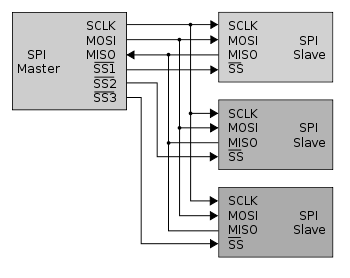
The protocol defines four different modes (0-3), which have to do with which SCLK edge the data is clocked on (rising or falling) and the SCLK inactive state (high or low). Mode 0 will work fine for the SPI experiments in this section.
The master and slave connects the shift registers in a ring, see picture below. The shift registers are 8 bits long in the picture but in principle they can be other lengths also. 12-bit and 16-bit lengths are also commonly used. The most significant bit (MSB) is typically sent first on the MOSI/MISO data lines. Note that this structure results in that the master receives one byte from the slave when one byte is sent.
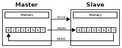
There is no specific upper frequency for the SCLK frequency. It depends on the SPI peripheral block in the microcontroller, the external SPI slave chip(s) and how far away the master and slaves(s) is/are. For breadboard experiments, the SCLK frequency should typically not exceed 1MHz. With proper pcb layout a frequency up to 20-30 MHz should not be a problem (assuming the chips involved support this frequency).
For more information about SPI, see http://en.wikipedia.org/wiki/Serial_Peripheral_Interface_Bus
Information
When working on breadboard signal frequencies cannot be too high. A good rule of thumb is to keep signal frequencies below 1MHz. A breadboard is simply not a good place for high frequency electronics. Decoupling capacitors should be used in all circuits but are sometimes ignored on breadboard setups - like in this experiment. A decoupling capacitor is placed as close as possible to the supply pins on an integrated circuit. It reduce voltage dips on the supply voltage.
Have a look in chapter 17 - LPC800 SPI0/1 with SSP in the LPC800 user’s manual for a description of how the SSP block works. SSP (Synchronous Serial Port) is NXP’s peripheral block that is capable of SPI communication (plus some other formats that will not be investigated in this experiment). There are two SSP blocks and anyone of them can be used since the flexible pinning of the LPC800 family makes it possible to assign the SSP signals to any pin.
Further, we will use a GPIO signals for SSEL. It is possible to use the SSEL signal from the SSP-block directly, but in order to make the code general and supporting multiple SPI slaves we will control the SSEL signals with a GPIO signal instead.
The mbed library provides a SPI class:
Import library
Public Member Functions |
|
| SPI (PinName mosi, PinName miso, PinName sclk) | |
|
Create a
SPI
master connected to the specified pins.
|
|
| void | format (int bits, int mode=0) |
|
Configure the data transmission format.
|
|
| void | frequency (int hz=1000000) |
|
Set the spi bus clock frequency.
|
|
| virtual int | write (int value) |
|
Write to the
SPI
Slave and return the response.
|
|
1) Hardware
In this lab you will need:
- 1x breadboard
- 9x 330 ohm resistor
- 1x 7-segment display
- 1x shift register (74HC595)
- cables
Mount the components on the breadboard and connect the breadboard to the LPC812 as show in the image below.
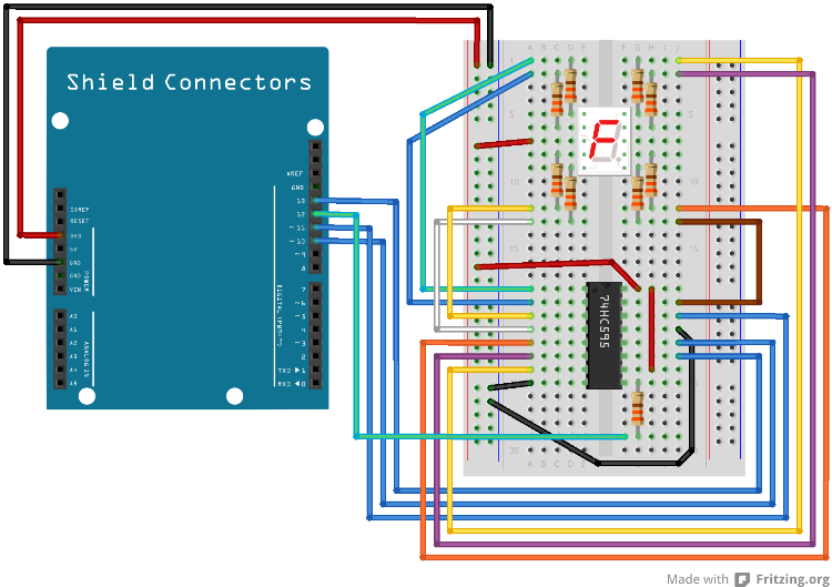
The pin(s) are specified in the mbed library with the actual pin names as well as some useful aliases:
| Schematic Name | mbed Pin Name | Arduino Shield Alias | Description |
|---|---|---|---|
| PIO0_12 | P0_12 | D13 | SPI SCK |
| PIO0_13 | P0_13 | D10 | Digital out used as SSEL |
| PIO0_14 | P0_14 | D11 | SPI MOSI |
| PIO0_15 | P0_15 | D12 | SPI MISO |
1) Description
In this experiment a shift register, the 74HC595 chip, shall be connected to the SPI bus. A byte will be transmitted to the shift register and then read back. The external shift register can be seen as a one byte memory. Not very cost effective or high performance but in this experiment focus is on the principles and getting to know the SPI bus and the SSP peripheral block.
Create an application that send one byte (8 bits) and then reads it back. Verify that the read-back byte is correct. PIO0_13 as SSEL signal and do not forget to initialize this GPIO signal as an output and to also control the signal levels during SPI communication. It shall be high when no communication takes place. Pull the signal low before transmitting the byte and then pull it high after the transmission.
main.cpp
#include "mbed.h"

DigitalOut ssel(D10);
SPI spi(D11, D12, D13); // mosi, miso, sclk

static int send(int val)
{
    // control SSEL
    ...

    int oldval = spi.write(val);

    // control SSEL
    ...

   return oldval;
}

int main()
{
    // value to send
    int val = ...;

    int dummy = send(val);
    int expected = send(0x00);

   // verify return value
}
It is now time to revisit the "Control 7-segment Display via Shift Register" experiment. In that experiment the SPI bus
was simulated in software. Now the SSP peripheral block shall be used for the SPI communication.
The MISO signal is no longer need since the content of the shift register is of no interest. Use PIO0_13 as SSEL signal and do not forget to initialize this GPIO signal as an output and to also control the signal levels during SPI communication, just like in the previous Lab.
2) Hardware
In this lab you will need:
- 1x breadboard
- 1x SPI E2PROM (25LC080)
- 1x 330 ohm resistor
- cables
Mount the components on the breadboard and connect the breadboard to the LPC812 as show in the image below.
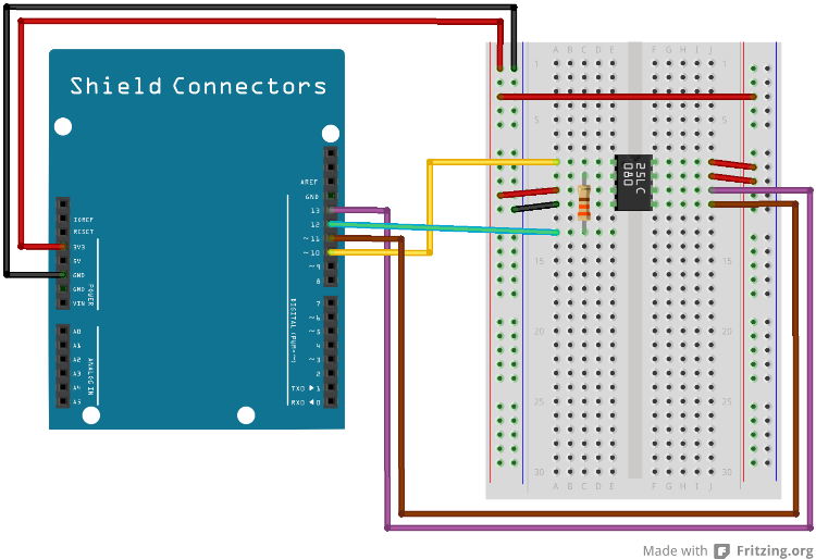
The pin(s) are specified in the mbed library with the actual pin names as well as some useful aliases:
| Schematic Name | mbed Pin Name | Arduino Shield Alias | Description |
|---|---|---|---|
| PIO0_12 | P0_12 | D13 | SPI SCK |
| PIO0_13 | P0_13 | D10 | Digital out used as SSEL |
| PIO0_14 | P0_14 | D11 | SPI MOSI |
| PIO0_15 | P0_15 | D12 | SPI MISO |
2) Description
In this experiment we will interface the 25LC080 chip, which is a 1024 byte serial E2PROM that directly interface the SPI bus. In this experiment signal P0_13 (Arduino shield pin name D10) is used as SSEL signal also in this experiment.
Have a look at the datasheet for the 25LC080 chip, for example here: http://ww1.microchip.com/downloads/en/DeviceDoc/22151b.pdf or search Microchip’s website if the link does not work.
The 25LC080 chip has a set of instructions. All SPI transmissions begin with the instruction to execute. The needed parameters (for the instruction) are then transmitted. The set of instructions are shown in the picture below (the picture comes from the 25LC080 datasheet).

To read in the memory region, a start address (16-bit address) is transmitted after the READ instruction. In total, three bytes are transmitted from the microcontroller to the 25LC080 chip before bytes can be read from the memory. As many bytes that are of interest can be read out in the read operation. An internal address counter is incremented after each transmitted byte. If the highest address is reached (0x03FF for this chip), the address counter rolls over to address 0x0000. Note that the SSEL signal (or CS that it is called in the picture below) is low during the complete operation.

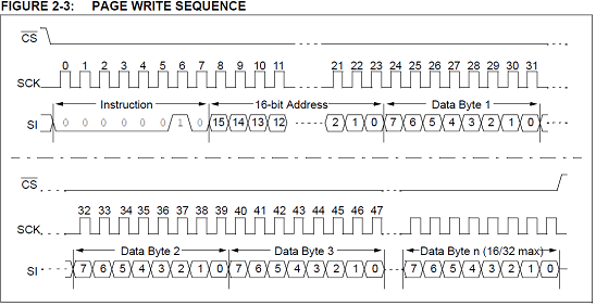
To write in the memory region, the WRITE instruction is used. Similar to the read operation, a 16-bit address is transmitted to set the start address of the write operation. One or many bytes can be written at the same time, see the pictures below.

Depending on chip version (C or D, check chip package marking for details), the maximum number of bytes to write is 16 or 32. Note that all bytes must be in the same page. Physical page boundaries start at addresses that are integer multiples of the page buffer size (16 or 32 bytes). It is for example allowed to write 7 bytes from address 4 to 10. It is not allowed to write 7 bytes from address 27 to 33 since a page boundary will then be crossed (true for both 16 and 32 byte page versions).
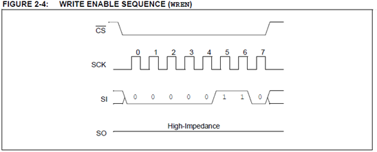
The 25LC080 chip contains a write enable latch. This latch must be set before any write operations are allowed. The WREN instruction sets the latch, i.e., enable a write operation. The WRDI operation resets the latch, i.e., block write operations. Note that the write enable bit must the set before every write operations. It is automatically reset after a successful write operation.
The WREN and WRDI instructions have no parameters. They are just one-byte instructions send to the 25LC080 chip. Note that the SSEL/CS signal must be brought high after the transmissions in order for the instructions to be actually executed. The WREN instruction is shown in the picture below. The WRDI instruction is similar and not shown.
There is also a status register. It can be read at any time, even during a write operation. It is possible to check the status of a write operation and detect when it is ready. It is also possible to read the write enable latch state as well as controlling write protection of blocks of the memory region. Read the datasheet for details.
Study the code below. It contains an initial framework for reading and writing to the 25LC080 chip:
SPI25LC080.h
#ifndef SPI25LC080_H
#define SPI25LC080_H

/**
 * Interface to the 25LC080 chip (http://ww1.microchip.com/downloads/en/DeviceDoc/22151b.pdf)
 *
 * @code
 * #include "mbed.h"
 *
 * SPI25LC080 e2prom;
 *
 * int main(void) {
 *    uint8_t buff[20];
 *    uint16_t addr = ...
 *
 *    while(1) {
 *       // read from e2prom
 *       e2prom.read(addr, buff, 20);
 *
 *       // write to e2prom
 *       e2prom.write(addr, buff, 20);
 *    }
 * }
 * @endcode
 */
class SPI25LC080 {
public:

    /** Create an interface to the 25LC080 chip
     *
     *  @param mosi the SPI MOSI pin
     *  @param sclk the SPI SCLK pin
     *  @param miso the SPI MISO pin
     */
    SPI25LC080(PinName mosi = P0_14, PinName sclk = P0_12, PinName miso = P0_15, PinName ssel = P0_13);

    /** Reads from the E2PROM
     *
     *  @param address the address to read from
     *  @param pBuf where to store the read data
     *  @param length the number of bytes to read
     */
    void read(uint16_t address, uint8_t* pData, uint32_t length);

    /** Writes to the E2PROM
     *
     *  @param address the address to write to
     *  @param pBuf the data to write
     *  @param length the number of bytes to write
     */
    void write(uint16_t address, uint8_t* pData, uint32_t length);

private:
    SPI        m_spi;
    DigitalOut m_ssel;
};

#endif
SPI25LC080.cpp
#include "mbed.h"
#include "SPI25LC080.h"

/* SPI E2PROM command set */
#define INST_WREN      0x06    /* MSB A8 is set to 0, simplifying test */
#define INST_WRDI      0x04
#define INST_RDSR      0x05
#define INST_WRSR      0x01
#define INST_READ      0x03
#define INST_WRITE     0x02

/* RDSR status bit definition */
#define RDSR_RDY       0x01
#define RDSR_WEN       0x02

/* Page size of E2PROM */
#define PAGE_SIZE        16

SPI25LC080::SPI25LC080(PinName mosi, PinName sclk, PinName miso, PinName ssel) :
    m_spi(mosi, miso, sclk), m_ssel(ssel)
{
}

void SPI25LC080::read(uint16_t address, uint8_t* pData, uint32_t length)
{
    //pull SSEL/CS low
    m_ssel = 0;

    //output read command and address
    m_spi.write(INST_READ);
    m_spi.write((address >> 8) & 0xff);
    m_spi.write(address & 0xff);

    //read bytes from E2PROM
    for (uint32_t i = 0; i < length; i++) {
        pData[i] = m_spi.write(0x00); // write dummy byte to get read next value
    }

    //pull SSEL/CS high
    m_ssel = 1;
}

void SPI25LC080::write(uint16_t address, uint8_t* pData, uint32_t length)
{
    //Insert code here to break up large write operation into several
    //page write operations...
    //Do not forget to add a 5ms delay after each page write operation!

    //pull SSEL/CS low
    m_ssel = 0;

    //output write command and address
    m_spi.write(INST_WRITE);
    m_spi.write((address >> 8) & 0xff);
    m_spi.write(address & 0xff);

    //send bytes to write to E2PROM
    for (uint32_t i = 0; i < length; i++) {
        m_spi.write(pData[i]);
    }

    //pull SSEL/CS high
    m_ssel = 1;
}
main.cpp
#include "mbed.h"
#include "SPI25LC080.h"

Serial pc(USBTX, USBRX);
SPI25LC080e2prom;

int main()
{
    //read from spi e2prom
    e2prom.read(...)

    //print read bytes
}
Add functionality in the write operation to check so that no page boundaries are crossed. Even better,
add functionality to break up a large write block to smaller, correctly addressed page writes. Do not
forget to add functionality in the write function to set the write enable latch before every write operation.
Create a program that writes a string and reads it back to verify that the write operation was successful. Also let the program print the content of the memory locations directly after power-up. By doing so it is also possible to verify that the SPI E2PROM is a non-volatile memory that keeps the content over a power cycle. Build the breadboard setup asd shown in the hardware section above and verify that it is possible to write and read in the memory region on the 25LC080 chip. Note that the 330 ohm series resistor on the MISO pin (pin 2 of the 25LC080) is not strictly needed. It is a safety precaution in case a faulty or wrong program executes on the LPC800, making the MISO pin an output in the LPC800. If this happens then the signal will have two drivers. This can cause damage to the respective pin drivers on the chips.
Solution(s)
Import programlpc812_exp_solution_spi-7-segment
Solutions for the SPI 7-Segment experiments for LPC812 MAX
Import programlpc812_exp_solution_spi-e2prom
Solutions for the SPI E2PROM experiments for LPC812 MAX
Please log in to post comments.
