Scaling Mbed's AOUT

The Mbed's AnalogOut pin can produce a voltage in the range 0v to 3.3v. However, often this range is not what is required for an end application. So some form of conversion is required to meet the specification that we have to work with.
The following presents two case studies. The first is the simplest. The second is an extension to this and represents a more real World example.
# 1. The Potential Divider.

This provides the simplest scaling from an input voltage to a lower output voltage. The relationship of Vin to Vout is simply calculated as
Vout = Vin * (R2 / R2 + R1)
So, for example, in the previous circuit diagram, if Vin = 10volts then:-
Vout = 10 * (3000 / 3000 + 2000)
Vout = 6volts.
Or, if Vin is connected to the MBed's P18 (AnalogOut) then the Vout range is:-
Vout = 3.3 * (R2 / R2 + R1)
Vout = 3.3 * 0.6
Therefore for 0v to 3.3v output from Mbed, Vout will be 0v to 1.98v
However, other than for the simplest of conversions the potential divider on it's own isn't going to be enough to reach what you have in your specification. For that, we'll need something a bit more complex but still easy to understand when broken down into it's parts.
# 2. The Active Output Stage (or analogue output buffer)
It may well be that your specification requires the AnalogOut to drive the audio in of some recording equipment that needs a signal in the range +/-1volt. Or perhaps you are controlling a DC servo amplifier that needs an input of +/-5v or +/-10v (common inputs for DC servo amplifiers). How are we going to get 0v to 3.3v into a Vout like that? Well, the following example is a typical design to get an audio out voltage of +/-1v as Vout.
In this case, we need to think of "scaling and offset" as "multiplication and addition". In the world of analogue electronics multiplication is known as amplification and addition is simply summing junctions. And fortunately for us, there's a really useful device that does both of these in one package, the Operational Amplifier (opamp).
First, lets begin with the circuit diagram for our output buffer. If you are new to this don't be put off by the circuit. Like all designs you can break it down into smaller parts that are easy to work with as this example will show.

Let's look at this circuit and break it down. First, Mbed's AnalogOut (P18) is connected to Vin. We are also going to need a reference voltage. More on this later, but for simplicity we will connect this to Mbed's 3.3v out on P40. And common is 0v GND (ground).
So, let's consider how we might use some math to convert 0 to 3.3 into -1 to +1. Well, to start with, in order to convert 0 to -1 we need to add -1 (minus one) so we know straight away we need an offset of -1. So, knowing the offset, what math do we need to convert 3 to +1? Well, we are adding -1 so we need to convert 3v into 2v, so we have a multiplication of 0.666r which, as you can see, is a division operation. In terms of the opamp, multiplication is the amplifiers gain. Gain's of less than 1 are actually "attenuators".
So, now we have a basic design criteria. This can now be translated into the circuit show above. As can be seen, Vin first meets the potential divider made up from R1 and R2. From the previous example we can calculate the value of these two resistors for 3.3 -> 1.0. Setting R1 to 68k and R2 to 27k we get V = 3.3 * (27/68+27) = 0.937v
Note, this isn't exactly 1v but it's close. We'll assume for now it's 1v and later we'll discuss error and how to mitigate or reduce error to an acceptable value.
So, the non-inverting input of the opamp will be 1v when the Mbed outputs 3.3v. We now need to "multiple by two and subtract one". This is where the amplifier's gain is setup and the offset is applied.
If you have read the above link to Wikipedia's page on opamps, you will be aware that the opamp's gain is set by the resistor combination Rf and Rg.
In the above circuit diagram, the feedback loop Rf is applied to the inverting input of the opamp. Combined with the resistor Rg the gain of the amplifier is therefore calculated thus:-
Av = 1 + Rf / Rg
So, if we make Rf and Rg = 10k (the same) the amplifiers gain is :-
Av = 1 + (10,000 / 10,000) = 2
So, with a gain of 2, the input signal applied to the non-inverting input is multipled by 2. Since we arranged for the potential divider from Vin to scale the voltage down from 3.3 to 1, the amplifier gain will multiple that to 2v. So we now have 0v -> 3.3v converted to 0v -> 2v. All we have to do now is subtract 1v to make this Vout -1 -> +1 range.
This is where the voltage reference comes in. In our simple example we connected Vref to the Mbed's 3.3v output. This is fed into a second potential divider R3 / R4. If we set R3 = 68k and R4 = 27k (the same values as the first potential divider) then the 3.3v will be scaled down to 1v. But it will always be 1v as the 3.3v from P40 never changes. This +1v is now fed, via Rg into the amplifiers inverting input. So this +1v signal is subtracted from Vout.
So, the Vout which was 0v -> 2v is now transformed to -1 -> +1v range. Bingo!
Design notes
The reader will already be aware that the conversion wasn't perfect but approximate due to errors. How do we manage or mitigate these errors? Well, first we have to understand where these errors come from. The most basic error is that off the shelf resistor values can't be purchased to exactly match the resistance values you calculate. They are sold in ranges of values. So you need to design around this. There are three basic ways. First, if your design specification includes an error by percentage (as it should) then you may fit straight in if you are lucky. For example if the spec says +/-1volt (+/-5%) then the above design may just fit into this requirement.
If it doesn't, you have two alternatives. You can create resistor networks with resistors in serial/parallel to arrive at a much closer overall resistance you need. Or you could fit a trimmer pot so that the reference voltage can be tweeked as needed. The dis-advantage of the later is that EVERY product you manufacture will need it's trimmer setup before shipping. That's a pita! ;)
One more consideration is the choice of opamp. In our design we had a gain of 2. This isn't huge and is closer to a unity gain (1) rather than a large gain. So when choosing an opamp you'll want one that works best in the unity gain region. And that's just the start. We haven't discussed frequency response, etc. That's really outside the scope of this short introductory article. The reader is advised to read up and learn about the characteristics of opamps.
Additionally, the opamp will need a +/- power rails. Often in digital designs the negative power rail is missing. In this case you'll need to provide a power rail for the opamp. Common methods are to use a DCDC converter.
Lastly, the voltage reference. In the example above we connected Vref to the Mbed's 3.3v on P40. In reality, this is a bad choice. Supply voltages often have a tiny "ripple" on them produced by all those transistors switching inside the LPC1768 and other parts of the system switching. This is what decoupling capacitors attempt to remove when placed close to an IC's power pins. However, you can't get rid of all of it. So using a power rail as a reference isn't good (Vout will have that ripple superimposed on it). A better choice is to use a dedicated reference voltage such as a LM4041 series device. However, if your spec isn't tight and a small amount of ripple is ok then a power rail maybe ok. But consider controlling a DC servo motor. Just imagine while holding the motor in one torque/current controlled position it vibrates madly. You may spend hours looking for a mistake in your choices of P, I or D or in fact your implementation of the PID. Only then to find that it's just noise on your reference voltage! Try to think ahead at the design stage where small simple variable mistakes can bite you in the butt later on :)
1 comment on Scaling Mbed's AOUT:

Please log in to post comments.
Hi Andy –
I enjoyed reading your article on scaling mbed’s AOUT. The illustrations are clear, and people looking for a tutorial on the subject should easily grasp your explanation.
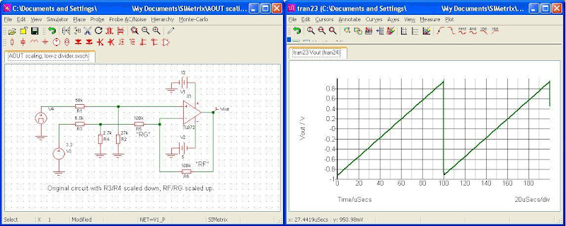
I believe, however, that the circuit will not operate quite as expected, for reasons that I will describe. You can see this by looking at the simulated output for the original circuit, shown below:
It is clear that the signal does not go to the desired –1.00 volt bottom level, and its peak-to-peak amplitude is a bit low. These problems arise from interaction between the feedback resistors (Rf and Rg), and the Vref scaling network (R3 and R4). Because these four resistors have values of roughly the same magnitude, there will be loading effects that are significant.
Consider the case of forward gain as seen by the (scaled) AOUT signal. Ideally, the gain is (1 + 10K/10K), or 2, as stated in the text. But that is only true if Rg is connected directly to ground. In reality, the path to ground is through R3 in parallel with R4 – which is about 19K ohms. So effectively Rg = 10K + R3||R4, or about 29K; and the corresponding
Av = (1 + 10/29), or about 1.3, not the expected 2.0.
With this gain, the peak-to-peak amplitude will be lower than desired.
A similar thing happens in the Vref path, as R4 of the voltage divider gets loaded by Rg going to a virtual ground (the negative input of an inverting amplifier may be considered a “virtual ground” node).
So the voltage division ratio is
Vref Ratio = (R4||Rg)/[R3 + (R4||Rg)], or 1/10.3,
rather than the expected 1/3.5. This means that we don’t subtract as much voltage as expected – the negative peak value will be 3.3 volts/10.3, or about -320 mV.
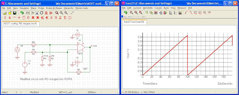
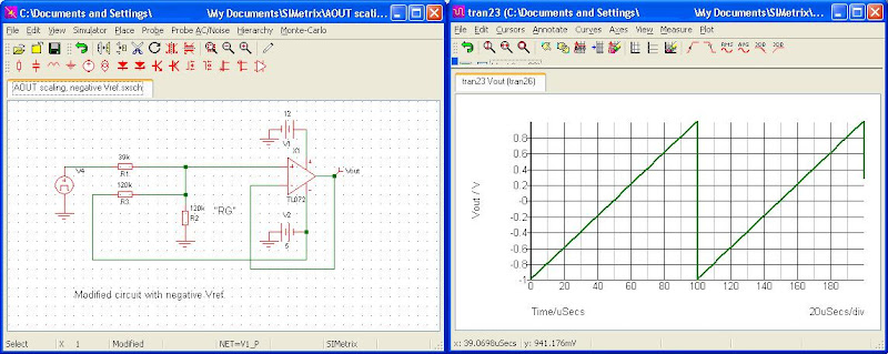
So the output isn’t all that close to the ideal case. But there are ways to address this. I’ll look at three alternatives in follow-up posts.