New VGA 640x400 70Hz library

24 Jul 2011

Just been skimming through this article, very good work, but how do you get data into the buffer, And what hardware & connections are you using ? I see you using I2S, but I have not found any nice clear examples.

Are you using a shift registor ? Also what screen ? I have a PSP display, that I have almost got working. But cannot get refresh rate anywhere near quick enough.

Cheers Ceri

24 Jul 2011

Quote:

These are the pins used:

DIP5 - Monochrome bitstream (connect to R, G and B through 1K resistors)

DIP8 - VSYNC

DIP25 - HSYNC

GND

DIP5 is the I2S output (that is the internal shift register output) You can connect a standard 640x480 (or better) VGA monitor. To get some more brightness you can lower the resistors to 390 without risk.

Your PSP screen needs parallel data, not serial so you need to de-serialize the data from the I2S output by using an external shift register. (The I2S output runs here at 25 Mbit/sec.)

The buffers are filled with pixel data which is coming from the fonttable which uses the textbuffer as input data. This way you can generate 640x400 pixeldata from a 2 kilobyte (text)buffer. You are limited to displaying the 256 shapes in the fonttable though.

I modified Ivo's text version to a full graphic version, this uses up 32000(!) bytes for the framebuffer but then each pixel is individually adressable.

As I said earlier, there is not enough ram in the mbed to do full colour graphic: 640x400 with 16 bits per pixel would need 512000 bytes.

24 Jul 2011
24 Jul 2011
25 Jul 2011

Wow, impressive work! I will try this project tonight. Is DIP5 means MBED pin-5 (SPI MOSI pin)? So, do you connect these R,G,B (through 1K resistors) to just one pin?

25 Jul 2011

Yes the output is monochrome only so you connect each of the R,G and B inputs of the VGA monitor with a resistor (anything between 390R and 1k depending on brightness) to the I2S output pin of the mbed. Or use green only for a nice nostalgic look :-)

Don't forget to connect some vga ground pins to the gnd of the mbed.

The main thing with this VGA library is that you still have a lot of CPU power left to do other things. Only problem so far is that filetransfer to the local filesystem will disrupt the screen (it stops the interupts). Using an external SD card however works without problems.

25 Jul 2011

/media/uploads/gertk/_scaled_2011-07-25_20.45.22.jpg /media/uploads/gertk/_scaled_2011-07-25_20.45.06.jpg /media/uploads/gertk/_scaled_2011-07-25_20.45.41.jpg 
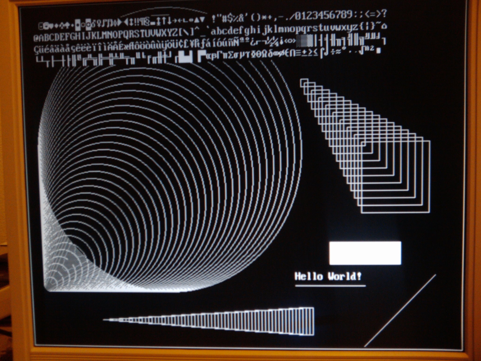
some screenshots from the demo

I bet these look good on a wide screen monitor :-) 640x400 does not equal square pixels on 4:3...

26 Jul 2011

Where can I get the VGA basic (timing, how to drive VGA, etc)? Cause I succeeded building this but I can't understand exactly what your codes did. Thank you. :)

26 Jul 2011

And, how can I communicate with another device with p27,p28 i2c? It makes my monitor gets no signal when I add another i2c command.

26 Jul 2011

These are the pins used:

DIP5 - Monochrome bitstream, connect to Red (VGA pin 1), Green (VGA pin 2) and Blue (VGA pin 3) through 1K resistors.

DIP8 - VSYNC (VGA pin 14)

DIP25 - HSYNC (VGA pin 13)

GND (VGA PIN 6, 7, 8)

The pixel timing as well as the sync timing is based on the first PWM and is set to a total of 800 clock cycles of 25 MHz. The I2S interface pushes out the bitstream and is also running at 25 Mhz. The I2S clock and wordselect signals are not used but these pins can be active. (note: the mbed is set to 100 MHz instead of 96 Mhz) Every time the first PWM resets it generates an interrupt and the I2S DMA sequence is started: first sending 640 pixels of active screen data, after that it sends some blank data which is automatically repeated by the I2S interface until the next interrupt.

// main PWM
    fl_pwm_set_match(0, 800);   // 800 color clocks

    // generate line interrupts from PWM MR0
    fl_pwm_config_match(0, FL_ON, FL_ON, FL_OFF);   // interrupt, reset, !stop

    // this PWM generates the HSYNC pulse
    fl_pwm_set_match(2, 16+HSHIFT);         // go low at 16
    fl_pwm_set_match(1, 48+HSHIFT);         // go high at 48
    fl_pwm_config_edges(2, FL_DOUBLE_EDGE); // need this for negative sync
    fl_pwm_output_enable(2, FL_ENABLE);     // enable this output

By default Ivo's original library switches off all peripherals of the mbed, I left that in. By activating/initializing a peripheral function after init_vga() they should come up as normal, for example I used the USB serial port and SPI interface without problems:

   init_vga();

    // serial port on at 115200 baud
    linktopc.baud(115200);
    setbuf(stdout, NULL); // no buffering for this filehandle

    // init SD card storage 
    SDFileSystem sd(p11, p12, p13, p14, "sd"); // mosi, miso, sclk, cs
26 Aug 2011

I updated the 640x400 demo and library into a new 640x480 full graphic and simplified the driver even more. It now uses some defines (like the Modelines for VGA) and the blank state is not needed anymore. You can still select the 640x400 mode.

By adding a small second framebuffer of 6400 bytes (6400/80 = 80 lines) you can now use full 640x480 @ 60 Hz. Squares and circles look a lot better now (at least on a 4:3 monitor)

demo program:

http://mbed.org/users/gertk/programs/vga640x480graphic/luzp3q

library:

http://mbed.org/users/gertk/libraries/vga640x480g/luz3p5

/media/uploads/gertk/_scaled_2011-07-27_21.54.24.jpg /media/uploads/gertk/2011-07-27_21.54.24.jpg

Enjoy!

30 Jul 2011

David Joseph Ariando wrote:

And, how can I communicate with another device with p27,p28 i2c? It makes my monitor gets no signal when I add another i2c command.

P27 and P28 are also on port0 so that might be the cause. I don't exactly know how the masking of the port pins is handled during DMA but it could also be that the I2C function is altering the port0 configuration or disables interrupts.

Gert

01 Aug 2011

Oh, Mr.Gert, I have succeeded, writing code after init_vga, as you said. I have a question. You made a code with serial communication to terminal, right? But I can't write anything from PC to my MBED VGA monitor.

03 Aug 2011

Quote:

Oh, Mr.Gert, I have succeeded, writing code after init_vga, as you said. I have a question. You made a code with serial communication to terminal, right? But I can't write anything from PC to my MBED VGA monitor.

If you insert this loop in the new 640x480g demo program instead of the last while(1) loop it will emulate a simple terminal. If you check out the code below I guess it will become clear how it works. You can add control codes for whatever function you want. Now it only responds to CR (13), LF (10) and FF (12) all other characters are put on screen literally. Note: there is no visible cursor.

  #define FONTHEIGHT 16
  #define FONTWIDTH 8

  int cursor_x=0;
  int cursor_y=0;
  int p;

  // simple terminal
  while (1) {
        p=getchar();  // get a character from the mbed USB serial interface
        switch (p) {  // check the character 
            case 13:  // CR ?
                cursor_x=0;           // reset cursor x to 0
                break;
            case 10:  // LF ?     
                cursor_y+=FONTHEIGHT; // add cursor y with fontheight
                if (cursor_y>479) {   // bottom edge ?
                    vga_scroll();     // do scroll
                    cursor_y=480-FONTHEIGHT; // rset cursor y to bottom line
                }
                cursor_x=0;           // reset cursor x 
                break;
            case 12: // FF ?
                vga_cls();            // clear the screen
                break;
            default: // all others
                vga_putchar(cursor_x,cursor_y,p,WHITE);  // put this character at cursor x,y
                cursor_x+=FONTWIDTH;                     // adjust x position 
                if (cursor_x>639) {                      // right edge ?
                    cursor_x=0;                          // if so reset to 0
                    cursor_y+=FONTHEIGHT;                // and adjust y position 
                    if (cursor_y>479) {                  // lower edge ?
                        vga_scroll();                    // scroll screen one character line up
                        cursor_y=480-FONTHEIGHT;         // reset cursor y to bottom line
                    }
                }
                break;
        }
    }
08 Aug 2011

Mr.Gert,

if I'm gonna use 400kHz I2C connection, can I just use code: i2c.frequency (400000); Or must I change the frequency because of the changing of MBED clock speed?

It's a bit confusing because init_vga code changes clock speed of MBED to 100MHz instead of 96MHz at normal speed.

08 Aug 2011

David Joseph Ariando wrote:

Mr.Gert,

if I'm gonna use 400kHz I2C connection, can I just use code: i2c.frequency (400000); Or must I change the frequency because of the changing of MBED clock speed?

It's a bit confusing because init_vga code changes clock speed of MBED to 100MHz instead of 96MHz at normal speed.

According to Ivo the initialisations of the uart and such should account for the higher clock speed of the CPU but I am not sure: at 115200 baud there are some errors during transmission so I guess the baudrate is a little bit off. You can either: leave out the PLL setting to 100 MHz (VGA timing will be a little bit off but I don't think that is a problem, or try and compensate the I2C timing. (although I2C is synchronous and should not cause problems) Just give it a try and let me know :-)

10 Aug 2011

If I am not mistaken, the CMSIS library uses the current core clock to set baud rates and other peripheral speed settings. As the mbed library is built on top of CMSIS, I assumed mbed objects to do the same. If in doubt, you can always set the peripheral speed again after initiating an object by calling the appropriate CMSIS or fastlib function (if the peripheral is yet supported by fastlib) and see if anything differs.

@Gert, I removed the uart0 initialization from my library (moved it to debug builds) as IMHO messing with the uart should not be part of a VGA library.

Also, I added some doxygen documentation today.

Regards, Ivo

10 Aug 2011

Could also be that the errors come from the fact that I used unbuffered serial. The less than 4% speed difference should not have that much influence on the baudrate.

@Ivo: did you try my latest 640x480g version ?

17 Aug 2011

Hello, I'm working on InterruptIn with this VGA mode. But since I use high speed InterruptIn (maybe 100KHz), I assumed it affects Timeout or Timer Interrupt in this VGA mode. So, I just have a blank VGA after seconds I reset my MBED.

Is there any method to set the InterruptIn priority next to other interrupts? I do think this will fix my problem. Or do you have any other methods?

regards, David Joseph.

17 Aug 2011

Well the PWM or DMA interrupt itself is about 30 to 35 kHz according to VGA line frequencies..

You can change priority with

NVIC_SetPriority( InterruptName, level )

level 255 is lowest priority, level 0 the highest

a list of interrupt handler names is at: http://mbed.org/forum/mbed/topic/383/?page=1#comment-2051 I guess you just leave off the 'Handler' part and it should give you the name of the Interrupt. Depending on which library you use you need to prioritize DMA_IRQ or PWM1_IRQ and the interrupt of your choice.

23 Aug 2011

Oh, thank you Mr.Gert, I have succeeded setting the IRQ. I should leave off the 'Handler' part and give 'n' as subtitute and it works.

I want to give a question from this code below:

  • (FL_PINMODE_OD0 + port) &= ( 1U << pin);

what's the meaning of "1U". I'm trying to understand all of the code used here. Thank you.

23 Aug 2011

And if you don't mind, would you describe how this code works:

#define FL_NVIC_INTERRUPT_FUNC(x, y) \
    static inline void fl_nvic_interrupt_##x(const unsigned interrupt) { \
        if (interrupt < 32) *FL_NVIC_##y##0 |= 1U<<interrupt;            \
        else                *FL_NVIC_##y##1 |= 1U<<(interrupt-32);       \
    } \
    static inline unsigned fl_nvic_interrupt_##x##_status(const unsigned interrupt) { \
        if (interrupt < 32) return (*FL_NVIC_##y##0) & (1U<<interrupt);               \
        else                return (*FL_NVIC_##y##1) & (1U<<(interrupt-32));          \
    }

I still quite don't understand what codes subtitute FL_NVIC_INTERRUPT_FUNC (x,y) when this code executed.

23 Aug 2011

1U is equal to ((unsigned)1).

The FL_NVIC_INTERRUPT_FUNC(x,y) macro defines two new functions each time it is evoked. For example:

FL_NVIC_INTERRUPT_FUNC(set_enable, ISER) expands to:

    static inline void fl_nvic_interrupt_set_enable(const unsigned interrupt) { \
        if (interrupt < 32) *FL_NVIC_ISER0 |= 1U<<interrupt;            \
        else                *FL_NVIC_ISER1 |= 1U<<(interrupt-32);       \
    } \
    static inline unsigned fl_nvic_interrupt_set_enable_status(const unsigned interrupt) { \
        if (interrupt < 32) return (*FL_NVIC_ISER0) & (1U<<interrupt);               \
        else                return (*FL_NVIC_ISER1) & (1U<<(interrupt-32));          \
    }

When such an inlined function is called, the compiler's optimization pass is assumed to reduce the function to a non-conditional statement (google for dead-code elimination and constant propagation if you want to read about the details).

25 Aug 2011

Thank you Mr.Ivo.

Here I'm trying to porting your code into a newbie language so I can understand how it works. But I cannot understand how this code works.

static const struct dma_lli blank_lli = {
    blanking, (void*)FL_I2STXFIFO, 0, 4
    | (1 << 12)
    | (1 << 15)
    | (2 << 18)
    | (2 << 21)
    | (0 << 26)
    | (0 << 27)
    | (0 << 31)
};

How could you set the control word with

    4
    | (1 << 12)
    | (1 << 15)
    | (2 << 18)
    | (2 << 21)
    | (0 << 26)
    | (0 << 27)
    | (0 << 31)

What was the meaning?

And if you please, could you tell me how this link list item made the I2S output keep on emitting zeroes even after DMA?

Thank you for your help.

Regards, David Joseph

This is what I called newbie code (not finished):

#include "mbed.h"

#define FL_PCON         ((volatile uint32_t *) 0x400FC0C0)  // Power Control Registers
#define FL_PCONP        ((volatile uint32_t *) 0x400FC0C4)  // Power Control For Peripheral Registers
#define FL_CLKSRCSEL    ((volatile uint32_t *) 0x400FC10C)  // Clock Source Select Register
#define FL_PCLKSEL0     ((volatile uint32_t *) 0x400FC1A8)  // Peripheral Clock Selection Register 0
#define FL_PCLKSEL1     ((volatile uint32_t *) 0x400FC1AC)  // Peripheral Clock Selection Register 1
#define FL_PLL0CON      ((volatile uint32_t *) 0x400FC080)  // PLL0 Control Register
#define FL_PLL0FEED     ((volatile uint32_t *) 0x400FC08C)  // PLL0 Feed Register (for changing in PLL0CON and PLL0CFG to take effect)
#define FL_PLL0STAT     ((volatile uint32_t *) 0x400FC088)  // PLL0 Status Register
#define FL_PLL0CFG      ((volatile uint32_t *) 0x400FC084)  // PLL0 Configuration Register
#define FL_CCLKCFG      ((volatile uint32_t *) 0x400FC104)  // CPU Clock Configuration Register

#define FL_PINSEL0      ((volatile uint32_t *) 0x4002c000)  // Pin Function Select Register 0
#define FL_PINSEL4      ((volatile uint32_t *) 0x4002c010)  // Pin Function Select Register 4
#define FL_PINMODE0     ((volatile uint32_t *) 0x4002c040)  // Pin Mode Select Register 0
#define FL_PINMODE4     ((volatile uint32_t *) 0x4002C050)  // Pin Mode Select Register 4
#define FL_PINMODE_OD2  ((volatile uint32_t *) 0x4002C070)  // Open Drain Pin Mode Select

#define FL_FIO0DIR      ((volatile uint32_t *) 0x2009C000)  // Fast GPIO Port Direction Control Register
#define FL_FIO0CLR      ((volatile uint32_t *) 0x2009C01C)  // Fast Port Output Set Register
#define FL_FIO0SET      ((volatile uint32_t *) 0x2009C018)  // Fast Port Output Set Register

#define FL_I2STXRATE    ((volatile uint32_t *) 0x400A8020)  // Transmit Clock Rate Register
#define FL_I2SDAO       ((volatile uint32_t *) 0x400A8000)  // Digital Audio Output Register
#define FL_I2STXFIFO    ((volatile uint32_t *) 0x400A8008)  // Transmit FIFO Register

#define FL_PWM1PR       ((volatile uint32_t *) 0x4001800C)  // PWM Prescale Register
#define FL_PWM1MR0      ((volatile uint32_t *) 0x40018018)  // PWM Match Register 0
#define FL_PWM1MR1      ((volatile uint32_t *) 0x4001801C)  // PWM Match Register 1
#define FL_PWM1MR2      ((volatile uint32_t *) 0x40018020)  // PWM Match Register 2
#define FL_PWM1MCR      ((volatile uint32_t *) 0x40018014)  // PWM Match Control Register
#define FL_PWM1PCR      ((volatile uint32_t *) 0x4001804C)  // PWM Control Register

#define FL_DMACConfig   ((volatile uint32_t *) 0x50004030)  // DMA Configuration Register
#define FL_DMACC0SrcAddr ((volatile uint32_t *) 0x50004100) // DMA Channel 0 Source Register
#define FL_DMACC0DestAddr ((volatile uint32_t *) 0x50004104)// DMA Channel 0 Destination Address 
#define FL_DMACC0LLI    ((volatile uint32_t *) 0x50004108)  // DMA Channel 0 Link List Item Register


 // define structure for DMA linked lists
    struct dma_lli {
        void *source;
        void *dest;
        struct dma_lli *next;
        unsigned int control_word;
    };

    // some arbitrary blank data for I2S used for blanking
    // even after DMA the I2S output will keep on emitting zeroes (= blank)
    static unsigned char blanking[32]= {
        0,0,0,0,0,0,0,0,
        0,0,0,0,0,0,0,0,
        0,0,0,0,0,0,0,0,
        0,0,0,0,0,0,0,0
    };

    // preset our blanking DMA linked list
    extern const struct dma_lli blank_lli;

    // blank linked lists ends the DMA cycle (lli=0)
    static const struct dma_lli blank_lli = {
        blanking, (void*)FL_I2STXFIFO, 0, 4
        | (1 << 12)
        | (1 << 15)
        | (2 << 18)
        | (2 << 21)
        | (0 << 26)
        | (0 << 27)
        | (0 << 31)
    };


int main() {
    *FL_PCONP = 0;                              // power off all peripherals
    *FL_CLKSRCSEL = 1;                          // select main oscilator as the PLL0 clock source
    *FL_PLL0CON = 1;                            // disconnect PLL0
    *FL_PLL0FEED = 0xAA;
    *FL_PLL0FEED = 0x55;   // feed for PLL0CON changes
    while (*FL_PLL0STAT&(1U<<25));              // wait until PLL0CON changes
    *FL_PLL0CON = 0;                            // disabling PLL0
    *FL_PLL0FEED = 0xAA;
    *FL_PLL0FEED = 0x55;   // feed for PLL0CON changes
    while (*FL_PLL0STAT&(1U<<24));              // wait until PLL0CON changes
    *FL_PLL0CFG = (1U<<16 | 24U);               // set N = 2 and M = 25, but PLL0CFG number is set by (N-1) and (M-1) for this purpose
    *FL_PLL0FEED = 0xAA;
    *FL_PLL0FEED = 0x55;   // feed for PLL0CFG changes
    *FL_PLL0CON = 1;                            // enabling PLL0
    *FL_PLL0FEED = 0xAA;
    *FL_PLL0FEED = 0x55;   // feed for PLL0CON changes
    while (!(*FL_PLL0STAT&(1U<<24)));           // wait until PLL0CON changes
    *FL_CCLKCFG = 2;                            // set cpu divider with 3, number sent tu CCLKCFG is (N-2) where N = 3
    while (!(*FL_PLL0STAT&(1U<<26)));           // wait until PLL0 locked
    *FL_PLL0CON = 3;                            // connect PLL0
    while (!(*FL_PLL0STAT&(1U<<25)));           // wait until PLL0CON changes

    *FL_PCONP |= (1U<<15);                      // power up gpio
    *FL_PINSEL0 &= ~(3U<<12);                   // set port0.6 (DIP8) with gpio
    *FL_FIO0DIR |= (1U<<6);                     // set port0.6 (DIP8) with "output"
    *FL_FIO0CLR |= (1U<<6);                     // set port0.6 (DIP8) with "produce low output"

    *FL_PCONP |= (1U<<27);                      // power up i2s
    *FL_PCLKSEL1 |= (1U<<22);                   // select PCLK = CCLK
    *FL_PINSEL0 |= (1U<<14);                    // P0.7 = i2stx_clk
    *FL_PINSEL0 |= (1U<<16);                    // P0.7 = i2stx_ws
    *FL_PINSEL0 |= (1U<<18);                    // P0.7 = i2stx_sda
    *FL_I2STXRATE = 4U | (1U<<8);               // produce MCLK with X = 1, Y = 4
    *FL_I2SDAO = (00U | (0U<<2) | (7U<<6) );    // set 8-bit data i2s, stereo format, ws_halfperiod = 7 or ws 16clk period

    *FL_PCONP |= (1U<<6);                       // power up pwm1
    *FL_PCLKSEL0 |= (1U<<12);                   // select PCLK PWM = CCLK
    *FL_PINSEL4 |= (1U<<2);                     // activate pwm on port 2.1
    *FL_PINMODE4 &= ~(3U<<2);
    *FL_PINMODE4 |= (2U<<2);                   // port 2.1 no pull-up pull-down resistor settings
    *FL_PINMODE_OD2 |= (1U<<1);                 // port 2.1 open-drain mode
    *FL_PWM1PR |= 3U;                           // tc is incremented every PR+1 cycles of PCLK PWM, in this case every 4 PCLK PWM resulting 25MHz clock PWM
    *FL_PWM1MR0 = 800U;                         // 800 color clocks
    *FL_PWM1MCR &= ~(7U);
    *FL_PWM1MCR |= 3U;    // interrupt, reset, !stop for MR0
    *FL_PWM1MR2 = 16U;                          //
    *FL_PWM1MR1 = 48U;                          //
    *FL_PWM1PCR |= (1U<<2);                     // double edge controlled mode for PWM2 output
    *FL_PWM1PCR |= (1U<<10);                    // pwm 2 output enabled

    *FL_PCONP |= (1U<<29);                      // power up gpdma
    *FL_DMACConfig |= 1U;                       // enable DMA
    while (*FL_DMACConfig & 1) {};                // wait until DMA enabled
    *FL_DMACC0SrcAddr = 0x2007C000;              // source address is framebuffer, pointer to peripheral SRAM
    *FL_DMACC0DestAddr = *FL_I2STXFIFO;           // destination address is i2s tx fifo 8x32bit


    while (1) {

    }

}

25 Aug 2011

David Joseph Ariando wrote:

Thank you Mr.Ivo.

Here I'm trying to porting your code into a newbie language so I can understand how it works. But I cannot understand how this code works.

static const struct dma_lli blank_lli = {
    blanking, (void*)FL_I2STXFIFO, 0, 4
    | (1 << 12)
    | (1 << 15)
    | (2 << 18)
    | (2 << 21)
    | (0 << 26)
    | (0 << 27)
    | (0 << 31)
};

How could you set the control word with

    4
    | (1 << 12)
    | (1 << 15)
    | (2 << 18)
    | (2 << 21)
    | (0 << 26)
    | (0 << 27)
    | (0 << 31)

What was the meaning?

The bits are documented in the LPC1768 user manual, section 31.5.20, page 602.

In this case:

  • TransferSize = 4
  • SBSize = 4
  • DBSize = 4
  • SWidth = Word (32-bits)
  • DWidth = Word (32-bits)
  • No source increment
  • No dest increment
  • No terminal count interrupt.

BTW if you look at init_dma_controller() in my console mode version, you can see how to easily generate new control words and display them via the serial interface.

David Joseph Ariando wrote:

And if you please, could you tell me how this link list item made the I2S output keep on emitting zeroes even after DMA?

That's the nature of the I2S interface. If there is no input, it just keeps on emitting the last word, which is all zeroes in Gert's driver's case.

26 Aug 2011

Thank you Mr.Ivo.

Lately I have seen every detail of your code and I confuse about few things. Here is one. In:

static void init_i2s(void) {
    // I2S on P0.9 (DIP5)
    fl_power_i2s(FL_ON);
    fl_select_clock_i2s(FL_CLOCK_DIV1);                     // assume 100MHz
    fl_pinsel(0, 7, FL_FUNC_ALT1, FL_IGNORE, FL_IGNORE);    // I2STX_CLK
    fl_pinsel(0, 8, FL_FUNC_ALT1, FL_IGNORE, FL_IGNORE);    // I2STX_WS
    fl_pinsel(0, 9, FL_FUNC_ALT1, FL_IGNORE, FL_IGNORE);    // I2STX_SDA
    fl_i2s_set_tx_rate(1, 4);
    fl_i2s_output_set_config(FL_8BITS, FL_STEREO, 8, 0, 0, 0, 0);

}

You have set x = 1 and y = 4. With equation:

I2STXMCLK = PCLK_I2S * (X/Y) /2

and PCLK_I2S = CCLK = 100MHz, is it true you have I2STXMCLK = 100MHz * (1/4)/2 = 12.5 MHz? I have checked everywhere and not get 25MHz as you said in your code (for I2S). Where do I wrong?

Thank you.

26 Aug 2011

Hmm, I'm not sure what's happening here. I agree that the divider should be (1/2)/2. The LPC176x errata says the X/Y divider does not work correctly for PCLK_I2S > 74MHz. I assume this is a glitch. I must confess that I used trial and error to get this working :) Perhaps the extra /2 stage is not triggered if the input clock is too high.

26 Aug 2011

Oh, I see, that's the problem.

I realize that I2S has 8×32-bit transmit FIFO. But with register I2STXFIFO (0x400A8008), I could just access 32bit or 1 word. How could I access another 7x32 bit?

And if I adjust setting with 8-bit stereo, so that will be

byte-a | byte-b | byte-c | byte-d

with 8-bit each. According to my acknowledge, could I set random data, for example I set value in a-c-b-d direction and get FIFO a-c-b-d? Or will I get a-b-c-d?

Thank you Sir.

28 Aug 2011

Consider the I2STXFIFO memory address as the entry point of the FIFO queue. Each value you write to that address is added to the queue. You write to the _same_ address to add values to the queue.

write X, write Y, write Z....

queue --> Z, Y, X ---> output

I don't understand the second part of your question...

29 Aug 2011

Oh, thank you Mr.Ivo. I understand both of my questions now with your answer.

Why do you set transfer size with 20? Source & destination burst with 4? Source and destination width with 32? (I'm still quite don't understand cleary the difference between transfer size, burst size, and source/destination width. Maybe that's why I don't understand these numbers you write.)

Also I can't understand why have you set blanking with 32 char size. Cause I2STXFIFO is just 32-bit accessible, why don't you set blanking with just one word size?