Prototype Enclosure
 Adam Green.
0
replies
Adam Green.
0
replies
Overview
Up until recently I have been doing most of my mbed based development with a breadboard but sometimes I want to take my development out on the road. I decided to place the mbed device in an enclosure from Sparkfun with the peripherals that I most often use such as ethernet, microSD, and USB mini-B connector.
Bill of Materials

| Description | Sparkfun Link |
|---|---|
| mbed LPC1768 | http://www.sparkfun.com/products/9564 |
| microSD breakout | http://www.sparkfun.com/products/544 |
| USB Mini-B Breakout | http://www.sparkfun.com/products/9966 |
| RJ45 Ethernet MagJack | http://www.sparkfun.com/products/8534 |
| RJ45 Ethernet MagJack Breakout | http://www.sparkfun.com/products/8790 |
| SparkFun Project Case - Clear | http://www.sparkfun.com/products/8632 |
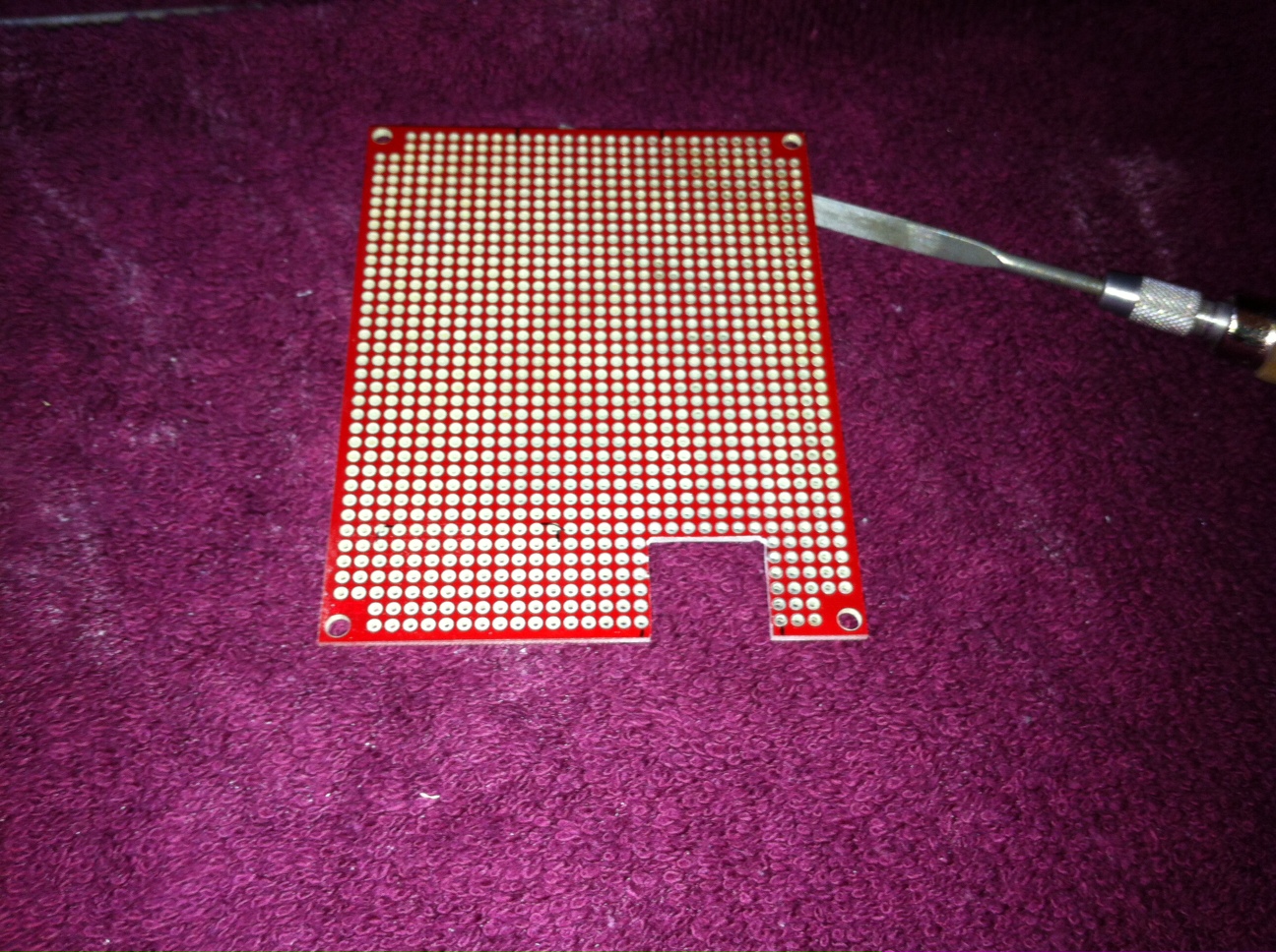
| ProtoBoard - Wombat | http://www.sparkfun.com/products/8619 |
| Mini Push Button Switch - Tall | http://www.sparkfun.com/products/8605 |
Construction
To make it easier to layout the parts on the PCB, I began by soldering the RJ-45 Ethernet jack into its breakout board.

The mbed 1768 microcontroller was mounted temporarily (to be soldered later) in the top row of the PCB, centered horizontally (8 holes on either side). Now that the mbed is mounted on PCB, it can be placed inside the case so that we can see where the USB programming port is located behind the back of the case. Since the case is clear, it is possible to see the programming port through the back of the case. This makes tracing the outline of the hole that is required in the case for the USB cable to fit through. I also marked a dot in the lower left hand corner of the case where a hole can be drilled for the reset button to pass through. The hole for this button is to be drilled low enough that the PCB can clear it when placed on the bottom standoffs.

I then temporarily placed the USB mini-B and RJ-45 breakout boards on the bottom of the PCB so that I could trace out their outlines.


Now it was down to the drill press to drill some holes into the case. First was to drill a 9/64" hole in the lower case for the reset button.

I then drilled a couple of 3/32" holes inside of the outline drawn earlier for the USB programming port. These two holes allow a file to fit and be used to refine the shape of the hole to the desired shape and size.


I used a Dremel with a cut-off wheel to rough out the slot for the RJ-45 breakout board and then refined it with a file so that the pins of the jack would clear through the PCB and allow the RJ45 breakout board to be mounted level with the PCB surface itself. The slot for the RJ45 jack was also aligned so that the holes in the breakout board would line up with the holes in the PCB while coming as close to flush as possible with the front bezel of the case.

Hot glue was then used to tack the reset push button into the lower case after two wires were soldered to the button.

To make it easier to remove the PCB completely from the case, the reset button isn't permanently attached to the mbed pins. Instead it has a 2-pin female header wired to the two wires coming from the reset switch and then a 2-pin right angle male header is soldered into the PCB. One pin of the male connector is connected to pin 1 - GND of the mbed and the other is connected to pin 4 - nR so that when the switch is closed, the reset signal will be pulled down to ground.

Warning
Initially I wired up the reset button just as I described above but then I had a problem that the mbed device would reset whenever there was a electro static discharge event within a few feet of the device. I got some great help from electrical engineers (Fenchurch and davidjh) on IRC and they gave me a bunch of good recommendations. Shorting the reset pin to Vout made the problem go away so I was dealing with an issue on this reset line. Adding a 0.1uF ceramic capacitor between GND and nR fixed the problem.

The RJ45 Ethernet Magjack Breakout board was then soldered onto the PCB. It was placed on the PCB over the slot that was previously cutout so that the pins on the bottom of the breakout board could protrude below the PCB and allow the breakout to lie directly on the PCB. The breakout was then connected to the PCB through the use of short pieces of solid gauge wire which had had its insulation removed. This breakout was then wired into the mbed device according to the table that follows. RJ45 Ethernet Breakout pins not mentioned in this table were left not connected. A set of twisted pair wires salvaged from an old CAT5 ethernet cable was used to connect the TD+/TD- and RD+/RD- signals.
| mbed pin | RJ45 Ethernet Breakout |
|---|---|
| GND | GS1 |
| VOUT | P3 and P6 |
| TD+ | P1 |
| TD- | P2 |
| RD+ | P7 |
| RD - | P8 |

With the PCB mounted in the case using the provided screws, the front bezel of the case was then laid in front and the location of the RJ45 jack marked. A slot was then cut in the bezel using a scroll saw and refined with a file until the RJ45 Ethernet jack fit well. The top of the case above the RJ45 jack also had to be filed down a bit to allow it to fit in smoothly.

To be continued...
Please log in to post comments.