Important changes to forums and questions
All forums and questions are now archived. To start a new conversation or read the latest updates go to forums.mbed.com.
11 years, 12 months ago.
circuit diagram
provide us the circuit diagram to interface potentiometer with emded board and program (i.e: taking analog input from potentiometer of 1 K , varies between 0-5V)
2 Answers
11 years, 11 months ago.
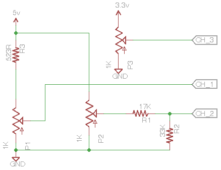
ceri provided good answers, I'm simply generating pictures - and adding a little discussion.

P2, R1, and R2 are what ceri described. The important factor is to keep the maximum voltage on the analog input at or below 3.3v. If the voltage goes above 3.3, it could damage the micro. When the wiper of P2 is at the top, you have a simple voltage divider of the 17k and the 33k where Vout = Vin * R2 / (R1 + R2) => 5 * 33 / (17 + 33) => 3.3v.
P1 and R3 do the same thing. Here it is 5 * 1000 / (523 + 1000) => 3.29v. The 0.01v difference is likely insignificant compared to the tolerance and linearity error of the potentiometer.
P3 shows the simplest solution. If the pot can be driven directly from the 3.3v supply which feeds the a/d, then you have no worry of over-voltage on the a/d pins.
Why choose one of these over the other? For most applications, the difference is insignificant. The series resistor R1 (17K) will limit the current flow that can get to the analog input. This is important if the 5v supply is not precise, or perhaps is an external 5v supply that could vary (so could be above 5v). On the other hand, the combination of P1 and R3 uses fewer parts, and P3 uses the fewest parts.