Breadboarding the LPC1768
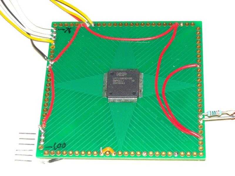
 Use of a LPC1768 device mounted on a double sided IC adapter
This experiment took place some time in 2016 and it seems like time to try to document it, especially as the circuit
- Illustrates how surprisingly easy to use the IC was
- gives access to the full pin-out of the IC
TQFP IC ADAPTER
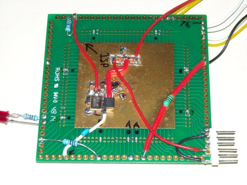
I believe the adapter was a ROTH RE934-07E. This has some extended pads on the IC side to enable use with smaller parts with lower pin-count. On the reverse side it has a large ground plane with positions for a 0603 size component between each lead and ground.

Power pins
0603-style zero-ohm links were fitted to all the designated ground pins of the IC: 11, 15, 31, 41, 55, 72, 83, 97
0603-style 10n (C0G) capacitors were fitted to all the designated supply pins of the IC: 10, 12, 19, 28, 42, 54, 71, 84, 96
The digital supply pins were common-ed using red wire: 28, 42, 54,71, 84, 96 (19 VBAT was left floating, as I may still add a battery)
The analog supply pin was connected to the digital via a small axial RF choke, 10uH.
Reset pin and ISP
Two 10K resistors were fitted in order to pull up the RESET and ISP lines. The Reset pin resistor goes from 17 to 28. The ISP resistor goes from 53 to 54. Switches were not fitted instead a temporary wire link was used to force ISP mode when needed. It is intended that future firmware builds will include code to detect the ISP start sequence and instigate IAP programming, however this has not been implemented.
Clock Oscillator
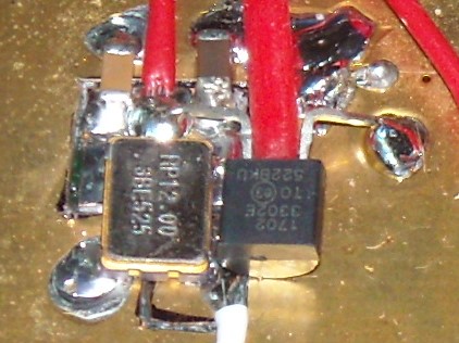
I recommend NOT trying to make a crystal work with an IC adapter. It probably would work though, 12MHz is an "easy" frequency, but the stray inductance and parallel tracks could easily disrupt it. The oscillator module is "safe".

The ground plane was cut in a few places to accommodate a clock oscillator (12MHz) and a 3.3V regulator (MCP1702-3302). To mount the oscillator two pads were cut out, one oversized one to accomodate terminals 1 and 4 and some DC supply bypass capacitors, and one smaller one to accomodate terminal 3. Oscillator terminal 2 is ground and is soldered straight to the uncut ground plane. The supply bypass capacitors are probably 100n and 10u.
The oscillator output is connected to the LPC1768 pin 22 via a 330pF capacitor. Note this probably should be 100pF.
Voltage Regulator
Microchip TO92 3.3V regulator. Watch the pin-out, elsewhere in plugblocks I've burned out two or three through getting the sequence wrong.
A power in pad was cut, then subsequently split in three to accomodate two diodes. The end result is the device can accept 5V in from USB or from a peripheral.
Serial Port
A small 6 way SIL connector was added to access serial port 0 using a FTDI USB-serial cable. I believe this is the 3.3V variant, however the positive pin is CONNECTED DIRECTLY TO USB VBUS and is definitely NOT 3.3V. I have used diodes before my regulator so power can be drawn from USB or from another 5V source.
The FTDI TTL-232R-3V3 connector
- Black Ground
- Brown not_CTS (in)
- Red VCC +5V
- Orange TXD (out)
- Yellow RXD (in)
- Green not_RTS (out)
Signal directions
- IN=LPC -> USB
- OUT=USB -> LPC
Pin 1 connects to ground Pin 2 is not connected Pin 3 connects to the voltage regulator via a diode Pin 4 connects to LPC pin 99 (RXD0) Pin 5 connects to LPC pin 98 (TXD0) Pin 6 is not connected
SPI port
This was built as an excercise, however having done it it seemed a shame not to use it. A connector was added to enable control of a Futaba GP9002A01 Vacuum fluorescent display module
GP9002 VFD port
Pinout of the 20 way display connector
- NC
- NC
- NC
- NC
- NC
- NC
- NC
- SO White To LPC pin 77 MISO1
- Black Ground
- INT Yellow To LPC pin 70 (P23)
- CLK White To LPC pin 78 SCK1
- SI White To LPC pin 76 MOSI1
- !CS Yellow To LPC pin 79 SSEL1
- C/!D Yellow To LPC pin 69 (P22)
- Red 5v (to LPC)
- NC
- Red 5V (from DC socket)
- Black Ground (to 20)
- Black Ground (from DC socket)
- Select Black Grounded (from 18)
Pin 20 selects serial mode. Using MBED SPI is usually FASTER than parallel unles you are prepared to code direct GPIO.
Notes on the GP9002A:
- The serial mode is bit-reversed relative to SPI. Some devices can select reverse bit order. I used a look-up-table.
- The GP9002A is capable of a greyscale mode as well as normal on-off mode. It isn't used much but worth it.
- According to the datasheet the GP9002A has built in fonts. I have never managed to make these work, the commands are ignored
- The display is FAST. There are no wait states, no busy polling.
Please log in to post comments.
