James Reynolds
/
AD594x Driver
Important changes to repositories hosted on mbed.com
Mbed hosted mercurial repositories are deprecated and are due to be permanently deleted in July 2026.
To keep a copy of this software download the repository Zip archive or clone locally using Mercurial.
It is also possible to export all your personal repositories from the account settings page.
Embed:
(wiki syntax)
Show/hide line numbers
ad5940.c
Go to the documentation of this file.
00001 /** 00002 * @file ad5940.c 00003 * @brief AD5940 library. This file contains all AD5940 library functions. 00004 * @author ADI 00005 * @date March 2019 00006 * @par Revision History: 00007 * 00008 * Copyright (c) 2017-2019 Analog Devices, Inc. All Rights Reserved. 00009 * 00010 * This software is proprietary to Analog Devices, Inc. and its licensors. 00011 * By using this software you agree to the terms of the associated 00012 * Analog Devices Software License Agreement. 00013 **/ 00014 #include "ad5940.h" 00015 00016 /*! \mainpage AD5940 Library Introduction 00017 * 00018 * 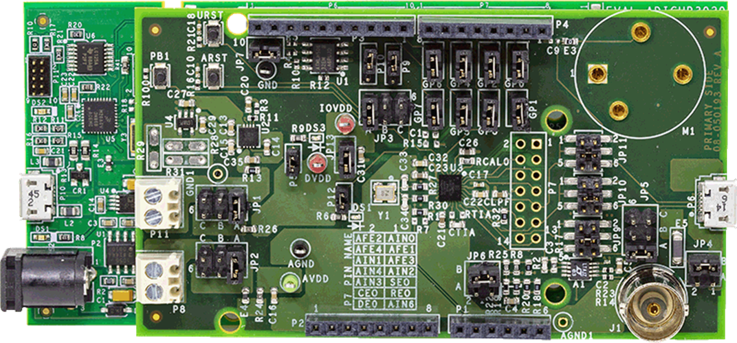 00019 * 00020 * # Introduction 00021 * 00022 * The documentation is for AD594x library and examples. 00023 * 00024 * # Manual Structure 00025 * 00026 * @ref AD5940_Library 00027 * - @ref AD5940_Functions 00028 * - @ref TypeDefinitions 00029 * @ref AD5940_Standard_Examples 00030 * @ref AD5940_System_Examples 00031 * 00032 * # How to Use It 00033 * We provide examples that can directly run out of box. 00034 * The files can generally be separated to three parts: 00035 * - AD5940 Library files. ad5940.c and ad5940.h specifically. These two files are shared among all examples. 00036 * - AD5940 System Examples. The system examples mean system level application like measuring impedance. 00037 * - Standard examples. These include basic block level examples like ADC. It shows how to setup and use one specific block. 00038 * 00039 * ## Requirements to run these examples 00040 * ### Hardware 00041 * - Use EVAL_AD5940 or EVAL_AD5941. The default MCU board we used is ADICUP3029. We also provide project for ST NUCLEO board. 00042 * - Or use EVAL_ADuCM355 00043 * ### Software 00044 * - Pull all the source file from [GitHub](https://github.com/analogdevicesinc/ad5940-examples.git) 00045 * - CMSIS pack that related to specific MCU. This normally is done by IDE you use. 00046 * 00047 * ## Materials 00048 * Please use this library together with following materials. 00049 * - [AD5940 Data Sheet](https://www.analog.com/media/en/technical-documentation/data-sheets/AD5940.pdf) 00050 * - [AD5940 Eval Board](https://www.analog.com/en/design-center/evaluation-hardware-and-software/evaluation-boards-kits/EVAL-AD5940.html) 00051 * 00052 */ 00053 00054 /* Remove below variables after AD594x is released. */ 00055 static BoolFlag bIsS2silicon = bFALSE; 00056 00057 /* Declare of SPI functions used to read/write registers */ 00058 #ifndef CHIPSEL_M355 00059 static uint32_t AD5940_SPIReadReg(uint16_t RegAddr); 00060 static void AD5940_SPIWriteReg(uint16_t RegAddr, uint32_t RegData); 00061 #else 00062 static uint32_t AD5940_D2DReadReg(uint16_t RegAddr); 00063 static void AD5940_D2DWriteReg(uint16_t RegAddr, uint32_t RegData); 00064 #endif 00065 00066 /** 00067 * @addtogroup AD5940_Library 00068 * The library functions, structures and constants. 00069 * @{ 00070 * @defgroup AD5940_Functions 00071 * @{ 00072 * @defgroup Function_Helpers 00073 * @brief The functions with no hardware access. They are helpers. 00074 * @{ 00075 * @defgroup Sequencer_Generator_Functions 00076 * @brief The set of function used to track all register read and write once it's enabled. It can translate register write operation to sequencer commands. 00077 * @{ 00078 */ 00079 00080 #define SEQUENCE_GENERATOR /*!< Build sequence generator part in to lib. Comment this line to remove this feature */ 00081 00082 #ifdef SEQUENCE_GENERATOR 00083 /** 00084 * Structure used to store register information(address and its data) 00085 * */ 00086 typedef struct 00087 { 00088 uint32_t RegAddr :8; /**< 8bit address is enough for sequencer */ 00089 uint32_t RegValue :24; /**< Reg data is limited to 24bit by sequencer */ 00090 }SEQGenRegInfo_Type; 00091 00092 /** 00093 * Sequencer generator data base. 00094 */ 00095 struct 00096 { 00097 BoolFlag EngineStart; /**< Flag to mark start of the generator */ 00098 uint32_t BufferSize; /**< Total buffer size */ 00099 00100 uint32_t *pSeqBuff; /**< The buffer for sequence generator(both sequences and RegInfo) */ 00101 uint32_t SeqLen; /**< Generated sequence length till now */ 00102 SEQGenRegInfo_Type *pRegInfo; /**< Pointer to buffer where stores register info */ 00103 uint32_t RegCount; /**< The count of register info available in buffer *pRegInfo. */ 00104 AD5940Err LastError; /**< The last error message. */ 00105 }SeqGenDB; /* Data base of Seq Generator */ 00106 00107 /** 00108 * @brief Manually input a command to sequencer generator. 00109 * @param CmdWord: The 32-bit width sequencer command word. @ref Sequencer_Helper can be used to generate commands. 00110 * @return None; 00111 */ 00112 void AD5940_SEQGenInsert(uint32_t CmdWord) 00113 { 00114 uint32_t temp; 00115 temp = SeqGenDB.RegCount + SeqGenDB.SeqLen; 00116 /* Generate Sequence command */ 00117 if(temp < SeqGenDB.BufferSize) 00118 { 00119 SeqGenDB.pSeqBuff[SeqGenDB.SeqLen] = CmdWord; 00120 SeqGenDB.SeqLen ++; 00121 } 00122 else /* There is no buffer */ 00123 SeqGenDB.LastError = AD5940ERR_BUFF; 00124 } 00125 00126 /** 00127 * @brief Search data-base to get current register value. 00128 * @param RegAddr: The register address. 00129 * @param pIndex: Pointer to a variable that used to store index of found register-info. 00130 * @return Return AD5940ERR_OK if register found in data-base. Otherwise return AD5940ERR_SEQREG. 00131 */ 00132 static AD5940Err AD5940_SEQGenSearchReg(uint32_t RegAddr, uint32_t *pIndex) 00133 { 00134 uint32_t i; 00135 00136 RegAddr = (RegAddr>>2)&0xff; 00137 for(i=0;i<SeqGenDB.RegCount;i++) 00138 { 00139 if(RegAddr == SeqGenDB.pRegInfo[i].RegAddr) 00140 { 00141 *pIndex = i; 00142 return AD5940ERR_OK; 00143 } 00144 } 00145 return AD5940ERR_SEQREG; 00146 } 00147 00148 /** 00149 * @brief Get the register default value by SPI read. This function requires AD5940 is in active state, otherwise we cannot get the default register value. 00150 * @param RegAddr: The register address. 00151 * @param pRegData: Pointer to a variable to store register default value. 00152 * @return Return AD5940ERR_OK. 00153 */ 00154 static AD5940Err AD5940_SEQGenGetRegDefault(uint32_t RegAddr, uint32_t *pRegData) 00155 { 00156 #ifdef CHIPSEL_M355 00157 *pRegData = AD5940_D2DReadReg(RegAddr); 00158 #else 00159 *pRegData = AD5940_SPIReadReg(RegAddr); 00160 #endif 00161 return AD5940ERR_OK; 00162 } 00163 00164 /** 00165 * @brief Record the current register info to data-base. Update LastError if there is error. 00166 * @param RegAddr: The register address. 00167 * @param RegData: The register data 00168 * @return Return None. 00169 */ 00170 static void AD5940_SEQRegInfoInsert(uint16_t RegAddr, uint32_t RegData) 00171 { 00172 uint32_t temp; 00173 temp = SeqGenDB.RegCount + SeqGenDB.SeqLen; 00174 00175 if(temp < SeqGenDB.BufferSize) 00176 { 00177 SeqGenDB.pRegInfo --; /* Move back */ 00178 SeqGenDB.pRegInfo[0].RegAddr = (RegAddr>>2)&0xff; 00179 SeqGenDB.pRegInfo[0].RegValue = RegData&0x00ffffff; 00180 SeqGenDB.RegCount ++; 00181 } 00182 else /* There is no more buffer */ 00183 { 00184 SeqGenDB.LastError = AD5940ERR_BUFF; 00185 } 00186 } 00187 00188 /** 00189 * @brief Get current register value. If we have record in data-base, read it. Otherwise, return the register default value. 00190 * @param RegAddr: The register address. 00191 * @return Return register value. 00192 */ 00193 static uint32_t AD5940_SEQReadReg(uint16_t RegAddr) 00194 { 00195 uint32_t RegIndex, RegData; 00196 00197 if(AD5940_SEQGenSearchReg(RegAddr, &RegIndex) != AD5940ERR_OK) 00198 { 00199 /* There is no record in data-base, read the default value. */ 00200 AD5940_SEQGenGetRegDefault(RegAddr, &RegData); 00201 AD5940_SEQRegInfoInsert(RegAddr, RegData); 00202 } 00203 else 00204 { 00205 /* return the current register value stored in data-base */ 00206 RegData = SeqGenDB.pRegInfo[RegIndex].RegValue; 00207 } 00208 00209 return RegData; 00210 } 00211 00212 /** 00213 * @brief Generate a sequencer command to write register. If the register address is out of range, it won't generate a command. 00214 * This function will also update the register-info in data-base to record current register value. 00215 * @param RegAddr: The register address. 00216 * @param RegData: The register value. 00217 * @return Return None. 00218 */ 00219 static void AD5940_SEQWriteReg(uint16_t RegAddr, uint32_t RegData) 00220 { 00221 uint32_t RegIndex; 00222 00223 if(RegAddr > 0x21ff) 00224 { 00225 SeqGenDB.LastError = AD5940ERR_ADDROR; /* address out of range */ 00226 return; 00227 } 00228 00229 if(AD5940_SEQGenSearchReg(RegAddr, &RegIndex) == AD5940ERR_OK) 00230 { 00231 /* Store register value */ 00232 SeqGenDB.pRegInfo[RegIndex].RegValue = RegData; 00233 /* Generate Sequence command */ 00234 AD5940_SEQGenInsert(SEQ_WR(RegAddr, RegData)); 00235 } 00236 else 00237 { 00238 AD5940_SEQRegInfoInsert(RegAddr, RegData); 00239 /* Generate Sequence command */ 00240 AD5940_SEQGenInsert(SEQ_WR(RegAddr, RegData)); 00241 } 00242 } 00243 00244 /** 00245 * @brief Initialize sequencer generator with specified buffer. 00246 * The buffer is used to store sequencer generated and record register value changes. 00247 * The command is stored from start address of buffer while register value is stored from end of buffer. 00248 * Buffer[0] : First sequencer command; 00249 * Buffer[1] : Second Sequencer command; 00250 * ... 00251 * Buffer[Last-1]: The second register value record. 00252 * Buffer[Last]: The first register value record. 00253 * @param pBuffer: Pointer to the buffer. 00254 * @param BufferSize: The buffer length. 00255 * @return Return None. 00256 */ 00257 void AD5940_SEQGenInit(uint32_t *pBuffer, uint32_t BufferSize) 00258 { 00259 if(BufferSize < 2) return; 00260 SeqGenDB.BufferSize = BufferSize; 00261 SeqGenDB.pSeqBuff = pBuffer; 00262 SeqGenDB.pRegInfo = (SEQGenRegInfo_Type*)pBuffer + BufferSize - 1; /* Point to the last element in buffer */ 00263 SeqGenDB.SeqLen = 0; 00264 00265 SeqGenDB.RegCount = 0; 00266 SeqGenDB.LastError = AD5940ERR_OK; 00267 SeqGenDB.EngineStart = bFALSE; 00268 } 00269 00270 /** 00271 * @brief Get sequencer command generated. 00272 * @param ppSeqCmd: Pointer to a variable(pointer) used to store the pointer to generated sequencer command. 00273 * @param pSeqLen: Pointer to a variable that used to store how many commands available in buffer. 00274 * @return Return lasterror. 00275 */ 00276 AD5940Err AD5940_SEQGenFetchSeq(const uint32_t **ppSeqCmd, uint32_t *pSeqLen) 00277 { 00278 AD5940Err lasterror; 00279 00280 if(ppSeqCmd) 00281 *ppSeqCmd = SeqGenDB.pSeqBuff; 00282 if(pSeqLen) 00283 *pSeqLen = SeqGenDB.SeqLen; 00284 00285 //SeqGenDB.SeqLen = 0; /* Start a new sequence */ 00286 lasterror = SeqGenDB.LastError; 00287 //SeqGenDB.LastError = AD5940ERR_OK; /* Clear error message */ 00288 return lasterror; 00289 } 00290 00291 /** 00292 * @brief Start or stop the sequencer generator. Once started, the register write will be recorded to sequencer generator. 00293 * Once it's disabled, the register write is written to AD5940 directly by SPI bus. 00294 * @param bFlag: Enable or disable sequencer generator. 00295 * @return Return None. 00296 */ 00297 void AD5940_SEQGenCtrl(BoolFlag bFlag) 00298 { 00299 if(bFlag == bFALSE) /* Disable sequence generator */ 00300 { 00301 SeqGenDB.EngineStart = bFALSE; 00302 } 00303 else 00304 { 00305 SeqGenDB.SeqLen = 0; 00306 SeqGenDB.LastError = AD5940ERR_OK; /* Clear error message */ 00307 SeqGenDB.EngineStart = bTRUE; 00308 } 00309 } 00310 00311 /** 00312 * @brief Calculate the number of cycles in the sequence 00313 * @return Return Number of ACLK Cycles that a generated sequence will take. 00314 */ 00315 uint32_t AD5940_SEQCycleTime(void) 00316 { 00317 uint32_t i, Cycles, Cmd; 00318 Cycles = 0; 00319 for(i=0;i<SeqGenDB.RegCount;i++) 00320 { 00321 Cmd = (SeqGenDB.pSeqBuff[i] >> 30) & 0x3; 00322 if (Cmd & 0x2) 00323 { 00324 /* A write command */ 00325 Cycles += 1; 00326 } 00327 else 00328 { 00329 if (Cmd & 0x1) 00330 { 00331 /* Timeout Command */ 00332 Cycles += 1; 00333 } 00334 else 00335 { 00336 /* Wait command */ 00337 Cycles += SeqGenDB.pSeqBuff[i] & 0x3FFFFFFF; 00338 } 00339 } 00340 } 00341 return Cycles; 00342 } 00343 #endif 00344 /** 00345 * @} Sequencer_Generator_Functions 00346 */ 00347 00348 /** 00349 * Check if an uint8_t value exist in table. 00350 */ 00351 static int32_t _is_value_in_table(uint8_t value, const uint8_t *table, uint8_t len, uint8_t *index) 00352 { 00353 for(int i=0; i<len; i++) 00354 { 00355 if(value == table[i]) 00356 { 00357 *index = i; 00358 return bTRUE; 00359 } 00360 } 00361 return bFALSE; 00362 } 00363 00364 /** 00365 * @brief return if the SINC3/SINC2 combination is available for notch 50Hz filter. 00366 * If it's not availabe, hardware automatically bypass Notch even if it's enabled. 00367 * @param pFilterInfo the filter configuration, only need sinc2/sinc3 osr and adc data rate information. 00368 * @return return bTRUE if notch 50Hz filter is available. 00369 */ 00370 BoolFlag AD5940_Notch50HzAvailable(ADCFilterCfg_Type *pFilterInfo, uint8_t *dl) 00371 { 00372 if((pFilterInfo->ADCRate == ADCRATE_800KHZ && pFilterInfo->ADCSinc3Osr == ADCSINC3OSR_2)||\ 00373 (pFilterInfo->ADCRate == ADCRATE_1P6MHZ && pFilterInfo->ADCSinc3Osr != ADCSINC3OSR_2)) 00374 { 00375 //this combination suits for filter: 00376 //SINC3 OSR2, for 800kSPS 00377 //and SINC3 OSR4 and OSR5 for 1.6MSPS, 00378 const uint8_t available_sinc2_osr[] = {ADCSINC2OSR_533, ADCSINC2OSR_667,ADCSINC2OSR_800, ADCSINC2OSR_889, ADCSINC2OSR_1333}; 00379 const uint8_t dl_50Hz[] = {15,12,10,9,6}; 00380 uint8_t index; 00381 if(_is_value_in_table(pFilterInfo->ADCSinc2Osr, available_sinc2_osr, sizeof(available_sinc2_osr), &index)) 00382 { 00383 *dl = dl_50Hz[index]; 00384 return bTRUE; 00385 } 00386 } 00387 else if(pFilterInfo->ADCRate == ADCRATE_1P6MHZ && pFilterInfo->ADCSinc3Osr == ADCSINC3OSR_2) 00388 { 00389 //this combination suits for filter: 00390 //SINC3 OSR2 for 1.6MSPS 00391 const uint8_t available_sinc2_osr[] = {ADCSINC2OSR_889, ADCSINC2OSR_1067, ADCSINC2OSR_1333}; 00392 const uint8_t dl_50Hz[] = {18,15,12}; 00393 uint8_t index; 00394 if(_is_value_in_table(pFilterInfo->ADCSinc2Osr, available_sinc2_osr, sizeof(available_sinc2_osr), &index)) 00395 { 00396 *dl = dl_50Hz[index]; 00397 return bTRUE; 00398 } 00399 } 00400 else if(pFilterInfo->ADCRate == ADCRATE_800KHZ && pFilterInfo->ADCSinc3Osr != ADCSINC3OSR_2) 00401 { 00402 //this combination suits for filter: 00403 //SINC3 OSR4 and OSR5 for 800kSPS, 00404 const uint8_t available_sinc2_osr[] = {ADCSINC2OSR_178, ADCSINC2OSR_267, ADCSINC2OSR_533, ADCSINC2OSR_640,\ 00405 ADCSINC2OSR_800, ADCSINC2OSR_1067}; 00406 const uint8_t dl_50Hz[] = {18,12,6,5,4,3}; 00407 uint8_t index; 00408 if(_is_value_in_table(pFilterInfo->ADCSinc2Osr, available_sinc2_osr, sizeof(available_sinc2_osr), &index)) 00409 { 00410 *dl = dl_50Hz[index]; 00411 return bTRUE; 00412 } 00413 } 00414 *dl = 0; 00415 return bFALSE; 00416 } 00417 00418 /** 00419 * @brief return if the SINC3/SINC2 combination is available for notch 60Hz filter. 00420 * If it's not availabe, hardware automatically bypass Notch even if it's enabled. 00421 * @param pFilterInfo the filter configuration, need sinc2/sinc3 osr and adc data rate information. 00422 * @return return bTRUE if notch 60Hz filter is available. 00423 */ 00424 BoolFlag AD5940_Notch60HzAvailable(ADCFilterCfg_Type *pFilterInfo, uint8_t *dl) 00425 { 00426 if((pFilterInfo->ADCRate == ADCRATE_800KHZ && pFilterInfo->ADCSinc3Osr == ADCSINC3OSR_2)||\ 00427 (pFilterInfo->ADCRate == ADCRATE_1P6MHZ && pFilterInfo->ADCSinc3Osr != ADCSINC3OSR_2)) 00428 { 00429 //this combination suits for filter: 00430 //SINC3 OSR2, for 800kSPS 00431 //and SINC3 OSR4 and OSR5 for 1.6MSPS, 00432 const uint8_t available_sinc2_osr[] = {ADCSINC2OSR_667, ADCSINC2OSR_1333}; 00433 const uint8_t dl_60Hz[] = {10,5}; 00434 uint8_t index; 00435 if(_is_value_in_table(pFilterInfo->ADCSinc2Osr, available_sinc2_osr, sizeof(available_sinc2_osr), &index)) 00436 { 00437 *dl = dl_60Hz[index]; 00438 return bTRUE; 00439 } 00440 } 00441 else if(pFilterInfo->ADCRate == ADCRATE_1P6MHZ && pFilterInfo->ADCSinc3Osr == ADCSINC3OSR_2) 00442 { 00443 //this combination suits for filter: 00444 //SINC3 OSR2 for 1.6MSPS 00445 const uint8_t available_sinc2_osr[] = {ADCSINC2OSR_889, ADCSINC2OSR_1333}; 00446 const uint8_t dl_60Hz[] = {15,10}; 00447 uint8_t index; 00448 if(_is_value_in_table(pFilterInfo->ADCSinc2Osr, available_sinc2_osr, sizeof(available_sinc2_osr), &index)) 00449 { 00450 *dl = dl_60Hz[index]; 00451 return bTRUE; 00452 } 00453 } 00454 else if(pFilterInfo->ADCRate == ADCRATE_800KHZ && pFilterInfo->ADCSinc3Osr != ADCSINC3OSR_2) 00455 { 00456 //this combination suits for filter: 00457 //SINC3 OSR4 and OSR5 for 800kSPS, 00458 const uint8_t available_sinc2_osr[] = {ADCSINC2OSR_178, ADCSINC2OSR_267, ADCSINC2OSR_533, ADCSINC2OSR_667,\ 00459 ADCSINC2OSR_889, ADCSINC2OSR_1333}; 00460 const uint8_t dl_60Hz[] = {15,10,5,4,3,2}; 00461 uint8_t index; 00462 if(_is_value_in_table(pFilterInfo->ADCSinc2Osr, available_sinc2_osr, sizeof(available_sinc2_osr), &index)) 00463 { 00464 *dl = dl_60Hz[index]; 00465 return bTRUE; 00466 } 00467 } 00468 *dl = 0; 00469 return bFALSE; 00470 } 00471 00472 /** 00473 * @brief Calculate how many clocks are needed in sequencer wait command to generate required number of data from filter output. 00474 * @note When measurement is done, it's recommend to disable blocks like ADCPWR, ADCCNV, SINC2, DFT etc. If blocks remain powered up, 00475 * they may need less clocks to generate required number of output. Use function @ref AD5940_AFECtrlS to control these blocks. 00476 * @param pFilterInfo: Pointer to configuration structure. 00477 * @param pClocks: pointer used to store results. 00478 * @return return none. 00479 */ 00480 void AD5940_ClksCalculate(ClksCalInfo_Type *pFilterInfo, uint32_t *pClocks) 00481 { 00482 uint32_t temp = 0; 00483 const uint32_t sinc2osr_table[] = {22,44,89,178,267,533,640,667,800,889,1067,1333,0}; 00484 const uint32_t sinc3osr_table[] = {5,4,2,0}; 00485 00486 *pClocks = 0; 00487 if(pFilterInfo == NULL) return; 00488 if(pClocks == NULL) return; 00489 if(pFilterInfo->ADCSinc2Osr > ADCSINC2OSR_1333) return; 00490 if(pFilterInfo->ADCSinc3Osr > 2) return; /* 0: OSR5, 1:OSR4, 2:OSR2 */ 00491 if(pFilterInfo->ADCAvgNum > ADCAVGNUM_16) return; /* Average number index:0,1,2,3 */ 00492 switch(pFilterInfo->DataType) 00493 { 00494 case DATATYPE_ADCRAW: 00495 temp = (uint32_t)(20*pFilterInfo->DataCount*pFilterInfo->RatioSys2AdcClk); 00496 break; 00497 case DATATYPE_SINC3: 00498 temp = (uint32_t)(((pFilterInfo->DataCount+2)*sinc3osr_table[pFilterInfo->ADCSinc3Osr]+1)*20*pFilterInfo->RatioSys2AdcClk + 0.5f); 00499 break; 00500 case DATATYPE_SINC2: 00501 temp = (pFilterInfo->DataCount+1)*sinc2osr_table[pFilterInfo->ADCSinc2Osr] + 1; 00502 pFilterInfo->DataType = DATATYPE_SINC3; 00503 pFilterInfo->DataCount = temp; 00504 AD5940_ClksCalculate(pFilterInfo, &temp); 00505 pFilterInfo->DataType = DATATYPE_SINC2; 00506 temp += 15; /* Need extra 15 clocks for FIFO etc. Just to be safe. */ 00507 break; 00508 case DATATYPE_NOTCH: 00509 { 00510 ADCFilterCfg_Type filter; 00511 filter.ADCRate = pFilterInfo->ADCRate; 00512 filter.ADCSinc3Osr = pFilterInfo->ADCSinc3Osr; 00513 filter.ADCSinc2Osr = pFilterInfo->ADCSinc2Osr; 00514 uint8_t dl=0, dl_50, dl_60; 00515 if(AD5940_Notch50HzAvailable(&filter, &dl_50)){ 00516 dl += dl_50 - 1; 00517 } 00518 if(AD5940_Notch60HzAvailable(&filter, &dl_60)){ 00519 dl += dl_60 - 1; 00520 } 00521 pFilterInfo->DataType = DATATYPE_SINC2; 00522 pFilterInfo->DataCount += dl; //DL is the extra data input needed for filter to output first data. 00523 AD5940_ClksCalculate(pFilterInfo,&temp); 00524 //restore the filter info. 00525 pFilterInfo->DataType = DATATYPE_NOTCH; 00526 pFilterInfo->DataCount -= dl; 00527 break; 00528 } 00529 case DATATYPE_DFT: 00530 switch(pFilterInfo->DftSrc) 00531 { 00532 case DFTSRC_ADCRAW: 00533 pFilterInfo->DataType = DATATYPE_ADCRAW; 00534 AD5940_ClksCalculate(pFilterInfo, &temp); 00535 break; 00536 case DFTSRC_SINC3: 00537 pFilterInfo->DataType = DATATYPE_SINC3; 00538 AD5940_ClksCalculate(pFilterInfo, &temp); 00539 break; 00540 case DFTSRC_SINC2NOTCH: 00541 if(pFilterInfo->BpNotch) 00542 pFilterInfo->DataType = DATATYPE_SINC2; 00543 else 00544 pFilterInfo->DataType = DATATYPE_NOTCH; 00545 AD5940_ClksCalculate(pFilterInfo, &temp); 00546 break; 00547 case DFTSRC_AVG: 00548 pFilterInfo->DataType = DATATYPE_SINC3; 00549 pFilterInfo->DataCount *= 1L<<(pFilterInfo->ADCAvgNum+1); /* 0: average2, 1: average4, 2: average8, 3: average16 */ 00550 AD5940_ClksCalculate(pFilterInfo, &temp); 00551 break; 00552 default: 00553 break; 00554 } 00555 pFilterInfo->DataType = DATATYPE_DFT; 00556 temp += 25; /* add margin */ 00557 break; 00558 default: 00559 break; 00560 } 00561 *pClocks = temp; 00562 } 00563 00564 /** 00565 @brief void AD5940_SweepNext(SoftSweepCfg_Type *pSweepCfg, float *pNextFreq) 00566 For sweep function, calculate next frequency point according to pSweepCfg info. 00567 @return Return next frequency point in Hz. 00568 */ 00569 void AD5940_SweepNext(SoftSweepCfg_Type *pSweepCfg, float *pNextFreq) 00570 { 00571 float frequency; 00572 00573 if(pSweepCfg->SweepLog)/* Log step */ 00574 { 00575 if(pSweepCfg->SweepStart<pSweepCfg->SweepStop) /* Normal */ 00576 { 00577 if(++pSweepCfg->SweepIndex == pSweepCfg->SweepPoints) 00578 pSweepCfg->SweepIndex = 0; 00579 frequency = pSweepCfg->SweepStart*pow(10,pSweepCfg->SweepIndex*log10(pSweepCfg->SweepStop/pSweepCfg->SweepStart)/(pSweepCfg->SweepPoints-1)); 00580 } 00581 else 00582 { 00583 pSweepCfg->SweepIndex --; 00584 if(pSweepCfg->SweepIndex >= pSweepCfg->SweepPoints) 00585 pSweepCfg->SweepIndex = pSweepCfg->SweepPoints-1; 00586 frequency = pSweepCfg->SweepStop*pow(10,pSweepCfg->SweepIndex* 00587 (log10(pSweepCfg->SweepStart/pSweepCfg->SweepStop)/(pSweepCfg->SweepPoints-1))); 00588 } 00589 } 00590 else/* Linear step */ 00591 { 00592 if(pSweepCfg->SweepStart<pSweepCfg->SweepStop) /* Normal */ 00593 { 00594 if(++pSweepCfg->SweepIndex == pSweepCfg->SweepPoints) 00595 pSweepCfg->SweepIndex = 0; 00596 frequency = pSweepCfg->SweepStart + pSweepCfg->SweepIndex*(double)(pSweepCfg->SweepStop-pSweepCfg->SweepStart)/(pSweepCfg->SweepPoints-1); 00597 } 00598 else 00599 { 00600 pSweepCfg->SweepIndex --; 00601 if(pSweepCfg->SweepIndex >= pSweepCfg->SweepPoints) 00602 pSweepCfg->SweepIndex = pSweepCfg->SweepPoints-1; 00603 frequency = pSweepCfg->SweepStop + pSweepCfg->SweepIndex*(double)(pSweepCfg->SweepStart - pSweepCfg->SweepStop)/(pSweepCfg->SweepPoints-1); 00604 } 00605 } 00606 00607 *pNextFreq = frequency; 00608 } 00609 00610 /** 00611 @brief Initialize Structure members to zero 00612 @param pStruct: Pointer to the structure. 00613 @param StructSize: The structure size in Byte. 00614 @return Return None. 00615 **/ 00616 void AD5940_StructInit(void *pStruct, uint32_t StructSize) 00617 { 00618 memset(pStruct, 0, StructSize); 00619 } 00620 00621 /** 00622 @brief Convert ADC Code to voltage. 00623 @param ADCPga: The ADC PGA used for this result. 00624 @param code: ADC code. 00625 @param VRef1p82: the actual 1.82V reference voltage. 00626 @return Voltage in volt. 00627 **/ 00628 float AD5940_ADCCode2Volt(uint32_t code, uint32_t ADCPga, float VRef1p82) 00629 { 00630 float kFactor = 1.835/1.82; 00631 float fVolt = 0.0; 00632 float tmp = 0; 00633 tmp = (int32_t)code - 32768; 00634 switch(ADCPga) 00635 { 00636 case ADCPGA_1: 00637 break; 00638 case ADCPGA_1P5: 00639 tmp /= 1.5f; 00640 break; 00641 case ADCPGA_2: 00642 tmp /= 2.0f; 00643 break; 00644 case ADCPGA_4: 00645 tmp /= 4.0f; 00646 break; 00647 case ADCPGA_9: 00648 tmp /= 9.0f; 00649 break; 00650 default:break; 00651 } 00652 fVolt = tmp*VRef1p82/32768*kFactor; 00653 return fVolt; 00654 } 00655 00656 /** 00657 * @brief Do complex number division. 00658 * @param a: The dividend. 00659 * @param b: The divisor. 00660 * @return Return result. 00661 **/ 00662 fImpCar_Type AD5940_ComplexDivFloat(fImpCar_Type *a, fImpCar_Type *b) 00663 { 00664 fImpCar_Type res; 00665 float temp; 00666 temp = b->Real*b->Real + b->Image*b->Image; 00667 res.Real = a->Real*b->Real + a->Image*b->Image; 00668 res.Real /= temp; 00669 res.Image = a->Image*b->Real - a->Real*b->Image; 00670 res.Image /= temp; 00671 return res; 00672 } 00673 00674 /** 00675 * @brief Do complex number multiplication. 00676 * @param a: The multiplicand. 00677 * @param b: The multiplier . 00678 * @return Return result. 00679 **/ 00680 fImpCar_Type AD5940_ComplexMulFloat(fImpCar_Type *a, fImpCar_Type *b) 00681 { 00682 fImpCar_Type res; 00683 00684 res.Real = a->Real*b->Real - a->Image*b->Image; 00685 res.Image = a->Image*b->Real + a->Real*b->Image; 00686 00687 return res; 00688 } 00689 /** 00690 * @brief Do complex number addition. 00691 * @param a: The addend. 00692 * @param b: The addend . 00693 * @return Return result. 00694 **/ 00695 fImpCar_Type AD5940_ComplexAddFloat(fImpCar_Type *a, fImpCar_Type *b) 00696 { 00697 fImpCar_Type res; 00698 00699 res.Real = a->Real + b->Real; 00700 res.Image = a->Image + b->Image; 00701 00702 return res; 00703 } 00704 00705 /** 00706 * @brief Do complex number subtraction. 00707 * @param a: The minuend. 00708 * @param b: The subtrahend . 00709 * @return Return result. 00710 **/ 00711 fImpCar_Type AD5940_ComplexSubFloat(fImpCar_Type *a, fImpCar_Type *b) 00712 { 00713 fImpCar_Type res; 00714 00715 res.Real = a->Real - b->Real; 00716 res.Image = a->Image - b->Image; 00717 00718 return res; 00719 } 00720 00721 /** 00722 * @brief Do complex number division. 00723 * @param a: The dividend. 00724 * @param b: The divisor. 00725 * @return Return result. 00726 **/ 00727 fImpCar_Type AD5940_ComplexDivInt(iImpCar_Type *a, iImpCar_Type *b) 00728 { 00729 fImpCar_Type res; 00730 float temp; 00731 temp = (float)b->Real*b->Real + (float)b->Image*b->Image; 00732 res.Real = (float)a->Real*b->Real + (float)a->Image*b->Image; 00733 res.Real /= temp; 00734 res.Image = (float)a->Image*b->Real - (float)a->Real*b->Image; 00735 res.Image /= temp; 00736 return res; 00737 } 00738 00739 /** 00740 * @brief Do complex number multiplication. 00741 * @param a: The multiplicand. 00742 * @param b: The multiplier . 00743 * @return Return result. 00744 **/ 00745 fImpCar_Type AD5940_ComplexMulInt(iImpCar_Type *a, iImpCar_Type *b) 00746 { 00747 fImpCar_Type res; 00748 00749 res.Real = (float)a->Real*b->Real - (float)a->Image*b->Image; 00750 res.Image = (float)a->Image*b->Real + (float)a->Real*b->Image; 00751 00752 return res; 00753 } 00754 00755 /** 00756 * @brief Calculate the complex number magnitude. 00757 * @param a: The complex number. 00758 * @return Return magnitude. 00759 **/ 00760 float AD5940_ComplexMag(fImpCar_Type *a) 00761 { 00762 return sqrt(a->Real*a->Real + a->Image*a->Image); 00763 } 00764 00765 /** 00766 * @brief Calculate the complex number phase. 00767 * @param a: The complex number. 00768 * @return Return phase. 00769 **/ 00770 float AD5940_ComplexPhase(fImpCar_Type *a) 00771 { 00772 return atan2(a->Image, a->Real); 00773 } 00774 00775 /** 00776 * @brief Calculate the optimum filter settings based on signal frequency. 00777 * @param freq: Frequency of signalr. 00778 * @return Return FreqParams. 00779 **/ 00780 FreqParams_Type AD5940_GetFreqParameters(float freq) 00781 { 00782 const uint32_t dft_table[] = {4, 8, 16, 32, 64, 128, 256, 512, 1024, 2048, 4096, 8192, 16384}; 00783 const uint32_t sinc2osr_table[] = {1, 22,44,89,178,267,533,640,667,800,889,1067,1333}; 00784 const uint32_t sinc3osr_table[] = {2, 4, 5}; 00785 float AdcRate = 800000; 00786 uint32_t n1 = 0; // Sample rate after ADC filters 00787 uint32_t n2 = 0; // Sample rate after DFT block 00788 uint32_t iCycle = 0; 00789 FreqParams_Type freq_params; 00790 /* High power mode */ 00791 if(freq >= 20000) 00792 { 00793 freq_params. DftSrc = DFTSRC_SINC3; 00794 freq_params.ADCSinc2Osr = 0; 00795 freq_params.ADCSinc3Osr = 2; 00796 freq_params.DftNum = DFTNUM_8192; 00797 freq_params.NumClks = 0; 00798 freq_params.HighPwrMode = bTRUE; 00799 return freq_params; 00800 } 00801 00802 if(freq < 0.51) 00803 { 00804 freq_params. DftSrc = DFTSRC_SINC2NOTCH; 00805 freq_params.ADCSinc2Osr = 6; 00806 freq_params.ADCSinc3Osr = 1; 00807 freq_params.DftNum = DFTNUM_8192; 00808 freq_params.NumClks = 0; 00809 freq_params.HighPwrMode = bTRUE; 00810 return freq_params; 00811 } 00812 00813 /* Start with SINC2 setting */ 00814 for(uint8_t i = 0; i<sizeof(sinc2osr_table) / sizeof(uint32_t); i++) 00815 { 00816 n1 = sinc2osr_table[i] * sinc3osr_table[1]; 00817 if(((AdcRate/n1) < freq * 10) && (freq<20e3)) 00818 continue; 00819 00820 /* Try DFT number */ 00821 for(uint32_t j = 8; j<sizeof(dft_table) / sizeof(uint32_t); j++) 00822 { 00823 n2 = dft_table[j]; 00824 iCycle = (uint32_t)(n1 * n2 * freq)/AdcRate; 00825 if(iCycle < 8) 00826 continue; 00827 freq_params. DftSrc = DFTSRC_SINC2NOTCH; 00828 freq_params.ADCSinc2Osr = i-1; 00829 freq_params.ADCSinc3Osr = 1; 00830 freq_params.DftNum = j; 00831 freq_params.NumClks = 0; 00832 freq_params.HighPwrMode = bFALSE; 00833 if(n1 == 4) 00834 { 00835 freq_params. DftSrc = DFTSRC_SINC3; 00836 freq_params.ADCSinc2Osr = 0; 00837 } 00838 return freq_params; 00839 } 00840 } 00841 00842 return freq_params; 00843 } 00844 00845 /** 00846 * @} Function_Helpers 00847 */ 00848 00849 #ifdef CHIPSEL_M355 00850 static void AD5940_D2DWriteReg(uint16_t RegAddr, uint32_t RegData) 00851 { 00852 if(((RegAddr>=0x1000)&&(RegAddr<=0x3014))) /* 32bit register */ 00853 *(volatile uint32_t *)(RegAddr+0x400c0000) = RegData; 00854 else /* 16bit register */ 00855 *(volatile uint16_t *)(RegAddr+0x400c0000) = RegData; 00856 } 00857 00858 static uint32_t AD5940_D2DReadReg(uint16_t RegAddr) 00859 { 00860 if(((RegAddr>=0x1000)&&(RegAddr<=0x3014))) /* 32bit register */ 00861 return *(volatile uint32_t *)(RegAddr+0x400c0000); 00862 else /* 16bit register */ 00863 return *(volatile uint16_t *)(RegAddr+0x400c0000); 00864 } 00865 00866 void AD5940_FIFORd(uint32_t *pBuffer, uint32_t uiReadCount) 00867 { 00868 while(uiReadCount--) 00869 *pBuffer++ = *(volatile uint32_t *)(0x400c206C); 00870 } 00871 #else 00872 /** 00873 * @defgroup SPI_Block 00874 * @brief Functions to communicate with AD5940 registers following AD5940 SPI protocols 00875 * @{ 00876 * 00877 * @defgroup SPI_Block_Functions 00878 * @brief The basic SPI protocols. All functions are basic on AD5940_ReadWriteNBytes which 00879 * provided by user. 00880 * 00881 * ##SPI basic protocol 00882 * All SPI protocol starts with one-byte command word. Following are data(16B or 32B) 00883 * There are four SPI commands available @ref SPI_Block_Const. 00884 * @{ 00885 */ 00886 00887 /** 00888 @brief Using SPI to transmit one byte and return the received byte. 00889 @param data: The 8-bit data SPI will transmit. 00890 @return received data. 00891 **/ 00892 static unsigned char AD5940_ReadWrite8B(unsigned char data) 00893 { 00894 uint8_t tx[1], rx[1]; 00895 tx[0] = data; 00896 AD5940_ReadWriteNBytes(tx,rx,1); 00897 return rx[0]; 00898 } 00899 00900 /** 00901 @brief Using SPI to transmit two bytes and return the received bytes. 00902 @param data: The 16-bit data SPI will transmit. 00903 @return received data. 00904 **/ 00905 static uint16_t AD5940_ReadWrite16B(uint16_t data) 00906 { 00907 uint8_t SendBuffer[2]; 00908 uint8_t RecvBuffer[2]; 00909 SendBuffer[0] = data>>8; 00910 SendBuffer[1] = data&0xff; 00911 AD5940_ReadWriteNBytes(SendBuffer,RecvBuffer,2); 00912 return (((uint16_t)RecvBuffer[0])<<8)|RecvBuffer[1]; 00913 } 00914 00915 /** 00916 * @brief Using SPI to transmit four bytes and return the received bytes. 00917 * @param data: The 32-bit data SPI will transmit. 00918 * @return received data. 00919 **/ 00920 static uint32_t AD5940_ReadWrite32B(uint32_t data) 00921 { 00922 uint8_t SendBuffer[4]; 00923 uint8_t RecvBuffer[4]; 00924 00925 SendBuffer[0] = (data>>24)&0xff; 00926 SendBuffer[1] = (data>>16)&0xff; 00927 SendBuffer[2] = (data>> 8)&0xff; 00928 SendBuffer[3] = (data )&0xff; 00929 AD5940_ReadWriteNBytes(SendBuffer,RecvBuffer,4); 00930 return (((uint32_t)RecvBuffer[0])<<24)|(((uint32_t)RecvBuffer[1])<<16)|(((uint32_t)RecvBuffer[2])<<8)|RecvBuffer[3]; 00931 } 00932 00933 /** 00934 * @brief Write register through SPI. 00935 * @param RegAddr: The register address. 00936 * @param RegData: The register data. 00937 * @return Return None. 00938 **/ 00939 static void AD5940_SPIWriteReg(uint16_t RegAddr, uint32_t RegData) 00940 { 00941 /* Set register address */ 00942 AD5940_CsClr(); 00943 AD5940_ReadWrite8B(SPICMD_SETADDR); 00944 AD5940_ReadWrite16B(RegAddr); 00945 AD5940_CsSet(); 00946 /* Add delay here to meet the SPI timing. */ 00947 AD5940_CsClr(); 00948 AD5940_ReadWrite8B(SPICMD_WRITEREG); 00949 if(((RegAddr>=0x1000)&&(RegAddr<=0x3014))) 00950 AD5940_ReadWrite32B(RegData); 00951 else 00952 AD5940_ReadWrite16B(RegData); 00953 AD5940_CsSet(); 00954 } 00955 00956 /** 00957 * @brief Read register through SPI. 00958 * @param RegAddr: The register address. 00959 * @return Return register data. 00960 **/ 00961 static uint32_t AD5940_SPIReadReg(uint16_t RegAddr) 00962 { 00963 uint32_t Data = 0; 00964 /* Set register address that we want to read */ 00965 AD5940_CsClr(); 00966 AD5940_ReadWrite8B(SPICMD_SETADDR); 00967 AD5940_ReadWrite16B(RegAddr); 00968 AD5940_CsSet(); 00969 /* Read it */ 00970 AD5940_CsClr(); 00971 AD5940_ReadWrite8B(SPICMD_READREG); 00972 AD5940_ReadWrite8B(0); //Dummy read 00973 /* The real data is coming */ 00974 if((RegAddr>=0x1000)&&(RegAddr<=0x3014)) 00975 Data = AD5940_ReadWrite32B(0); 00976 else 00977 Data = AD5940_ReadWrite16B(0); 00978 AD5940_CsSet(); 00979 return Data; 00980 } 00981 00982 /** 00983 @brief Read specific number of data from FIFO with optimized SPI access. 00984 @param pBuffer: Pointer to a buffer that used to store data read back. 00985 @param uiReadCount: How much data to be read. 00986 @return none. 00987 **/ 00988 void AD5940_FIFORd(uint32_t *pBuffer, uint32_t uiReadCount) 00989 { 00990 /* Use function AD5940_SPIReadReg to read REG_AFE_DATAFIFORD is also one method. */ 00991 uint32_t i; 00992 00993 if(uiReadCount < 3) 00994 { 00995 /* This method is more efficient when readcount < 3 */ 00996 uint32_t i; 00997 AD5940_CsClr(); 00998 AD5940_ReadWrite8B(SPICMD_SETADDR); 00999 AD5940_ReadWrite16B(REG_AFE_DATAFIFORD); 01000 AD5940_CsSet(); 01001 for(i=0;i<uiReadCount;i++) 01002 { 01003 AD5940_CsClr(); 01004 AD5940_ReadWrite8B(SPICMD_READREG); 01005 AD5940_ReadWrite8B(0);//Write Host status/Don't care 01006 pBuffer[i] = AD5940_ReadWrite32B(0); 01007 AD5940_CsSet(); 01008 } 01009 } 01010 else 01011 { 01012 AD5940_CsClr(); 01013 AD5940_ReadWrite8B(SPICMD_READFIFO); 01014 /* 6 dummy write before valid data read back */ 01015 for(i=0;i<6;i++) 01016 AD5940_ReadWrite8B(0); 01017 /* Continuously read DATAFIFORD register with offset 0 */ 01018 for(i=0;i<uiReadCount-2;i++) 01019 { 01020 pBuffer[i] = AD5940_ReadWrite32B(0); /*Offset is 0, so we always read DATAFIFORD register */ 01021 } 01022 /* Read back last two FIFO data with none-zero offset*/ 01023 pBuffer[i++] = AD5940_ReadWrite32B(0x44444444); 01024 pBuffer[i] = AD5940_ReadWrite32B(0x44444444); 01025 AD5940_CsSet(); 01026 } 01027 } 01028 01029 /** 01030 * @} SPI_Block_Functions 01031 * @} SPI_Block 01032 */ 01033 #endif 01034 01035 /** 01036 * @brief Write register. If sequencer generator is enabled, the register write is recorded. 01037 * Otherwise, the data is written to AD5940 by SPI. 01038 * @param RegAddr: The register address. 01039 * @param RegData: The register data. 01040 * @return Return None. 01041 **/ 01042 void AD5940_WriteReg(uint16_t RegAddr, uint32_t RegData) 01043 { 01044 #ifdef SEQUENCE_GENERATOR 01045 if(SeqGenDB.EngineStart == bTRUE) 01046 AD5940_SEQWriteReg(RegAddr, RegData); 01047 else 01048 #endif 01049 #ifdef CHIPSEL_M355 01050 AD5940_D2DWriteReg(RegAddr, RegData); 01051 #else 01052 AD5940_SPIWriteReg(RegAddr, RegData); 01053 #endif 01054 } 01055 01056 /** 01057 * @brief Read register. If sequencer generator is enabled, read current register value from data-base. 01058 * Otherwise, read register value by SPI. 01059 * @param RegAddr: The register address. 01060 * @return Return register value. 01061 **/ 01062 uint32_t AD5940_ReadReg(uint16_t RegAddr) 01063 { 01064 #ifdef SEQUENCE_GENERATOR 01065 if(SeqGenDB.EngineStart == bTRUE) 01066 return AD5940_SEQReadReg(RegAddr); 01067 else 01068 #endif 01069 #ifdef CHIPSEL_M355 01070 return AD5940_D2DReadReg(RegAddr); 01071 #else 01072 return AD5940_SPIReadReg(RegAddr); 01073 #endif 01074 } 01075 01076 01077 /** 01078 * @defgroup AFE_Control 01079 * @brief Some functions to control the whole AFE. They are top level switches. 01080 * @{ 01081 * @defgroup AFE_Control_Functions 01082 * The top-level control functions for whole AFE perspective. 01083 * @details This function set is used to control the whole AFE block by block. It's a top-level configuration. 01084 * It's convenient when do initialization work with the functions called BLOCK**Cfg**. You can tune the parameters at run-time using more detailed 01085 * functions from each block. rather than top-level functions where you need to configure all parameters. 01086 * @{ 01087 */ 01088 01089 /** 01090 * @brief Initialize AD5940. This function must be called whenever there is reset(Software Reset or Hardware reset or Power up) happened. 01091 * This function is used to put AD5940 to correct state. 01092 * @return return None 01093 **/ 01094 void AD5940_Initialize(void) 01095 { 01096 int i; 01097 /* Write following registers with its data sequentially whenever there is a reset happened. */ 01098 const struct 01099 { 01100 uint16_t reg_addr; 01101 uint32_t reg_data; 01102 }RegTable[]= 01103 { 01104 {0x0908, 0x02c9}, 01105 {0x0c08, 0x206C}, 01106 {0x21F0, 0x0010}, 01107 #ifndef CHIPSEL_M355 01108 /* This is AD5940 */ 01109 {0x0410, 0x02c9}, 01110 {0x0A28, 0x0009}, 01111 #else 01112 /* This is ADuCM355 */ 01113 {0x0410, 0x001a}, 01114 {0x0A28, 0x0008}, 01115 #endif 01116 {0x238c, 0x0104}, 01117 {0x0a04, 0x4859}, 01118 {0x0a04, 0xF27B}, 01119 {0x0a00, 0x8009}, 01120 {0x22F0, 0x0000}, 01121 // 01122 {0x2230, 0xDE87A5AF}, 01123 {0x2250, 0x103F}, 01124 {0x22B0, 0x203C}, 01125 {0x2230, 0xDE87A5A0}, 01126 }; 01127 //initialize global variables 01128 SeqGenDB.SeqLen = 0; 01129 SeqGenDB.RegCount = 0; 01130 SeqGenDB.LastError = AD5940ERR_OK; 01131 SeqGenDB.EngineStart = bFALSE; 01132 #ifndef CHIPSEL_M355 01133 AD5940_CsSet(); /* Pull high CS in case it's low */ 01134 #endif 01135 for(i=0; i<sizeof(RegTable)/sizeof(RegTable[0]); i++) 01136 AD5940_WriteReg(RegTable[i].reg_addr, RegTable[i].reg_data); 01137 i = AD5940_ReadReg(REG_AFECON_CHIPID); 01138 if(i == 0x5501) 01139 bIsS2silicon = bTRUE; 01140 else if(i == 0x5502) /* S3 chip-id is 0x5502. The is no difference with S2. */ 01141 bIsS2silicon = bTRUE; 01142 else if(i == 0x5500) 01143 bIsS2silicon = bFALSE; 01144 #ifdef ADI_DEBUG 01145 else 01146 { 01147 printf("CHIPID read error:0x%04x. AD5940 is not present?\n", i); 01148 while(1); 01149 } 01150 #ifdef CHIPSEL_M355 01151 ADI_Print("This ADuCM355!\n"); 01152 #else 01153 ADI_Print("This AD594x!\n"); 01154 #endif 01155 ADI_Print("Note: Current Silicon is %s\n", bIsS2silicon?"S2":"S1"); 01156 ADI_Print("AD5940LIB Version:v%d.%d.%d\n", AD5940LIB_VER_MAJOR, AD5940LIB_VER_MINOR, AD5940LIB_VER_PATCH); 01157 #endif 01158 } 01159 01160 /** 01161 * @brief Control most AFE digital and analog block within one register access. 01162 * @param AfeCtrlSet: A set of blocks that will be controlled select it from @ref AFECTRL_Const Below is two examples to use it. 01163 * - AFECTRL_HPREFPWR: Control high power reference(bandgap). 01164 * - AFECTRL_WG|AFECTRL_ADCPWR: The OR'ed control set. Control Waveform generator and ADC power. 01165 * @param State: Enable or disable selected control set signal. Select from @BoolFlag 01166 * - bFALSE: Disable or power down selected block(s). 01167 * - bTRUE: Enable all selected block(s). 01168 @return return none. 01169 */ 01170 void AD5940_AFECtrlS(uint32_t AfeCtrlSet, BoolFlag State) 01171 { 01172 /* Check parameters */ 01173 uint32_t tempreg; 01174 tempreg = AD5940_ReadReg(REG_AFE_AFECON); 01175 if (State == bTRUE) { 01176 /* Clear bits to enable HPREF and ALDOLimit*/ 01177 if (AfeCtrlSet & AFECTRL_HPREFPWR) { 01178 tempreg &= ~BITM_AFE_AFECON_HPREFDIS; 01179 AfeCtrlSet &= ~AFECTRL_HPREFPWR; 01180 } 01181 if(AfeCtrlSet & AFECTRL_ALDOLIMIT) 01182 { 01183 tempreg &= ~BITM_AFE_AFECON_ALDOILIMITEN; 01184 AfeCtrlSet &= ~AFECTRL_ALDOLIMIT; 01185 } 01186 tempreg |= AfeCtrlSet; 01187 } 01188 else 01189 { 01190 /* Set bits to Disable HPREF and ALDOLimit*/ 01191 if(AfeCtrlSet & AFECTRL_HPREFPWR) 01192 { 01193 tempreg |= BITM_AFE_AFECON_HPREFDIS; 01194 AfeCtrlSet &= ~AFECTRL_HPREFPWR; 01195 } 01196 if(AfeCtrlSet & AFECTRL_ALDOLIMIT) 01197 { 01198 tempreg |= BITM_AFE_AFECON_ALDOILIMITEN; 01199 AfeCtrlSet &= ~AFECTRL_ALDOLIMIT; 01200 } 01201 tempreg &= ~AfeCtrlSet; 01202 } 01203 AD5940_WriteReg(REG_AFE_AFECON, tempreg); 01204 } 01205 /** When LP mode is enabled, some functions are under control of LPMODECON, rather than original registers. */ 01206 /** @warning LPMODE is key protected, this function only takes effect after AD5940_LPModeEnS(bTRUE) */ 01207 /** 01208 * @brief For LP mode, use one register to control most AFE digital and analog block. 01209 * @details The parameter means the blocks. The selected block will be enabled. All others will be disabled. 01210 * The method to enable/disable blocks are defined by register LPMODECON, either by clearing or setting bits. 01211 * @param EnSet: A set of blocks that will be enabled. Select it from @ref LPMODECTRL_Const. All others not selected in EnSet will be disabled. 01212 * - LPMODECTRL_ALDOPWR|LPMODECTRL_HFOSCEN: Turn on ALDO and HFOSC, disable all others. 01213 * - LPMODECTRL_ALL: Enable all blocks. 01214 @return return none. 01215 */ 01216 AD5940Err AD5940_LPModeCtrlS(uint32_t EnSet) 01217 { 01218 /* Check parameters */ 01219 uint32_t tempreg; 01220 uint32_t DisSet; /* The blocks to be disabled */ 01221 DisSet = LPMODECTRL_ALL & (~EnSet); 01222 tempreg = AD5940_ReadReg(REG_AFE_LPMODECON); 01223 /* Enable selected set */ 01224 { 01225 /* Clear bits to enable HFOSC, HPREF, ALDO */ 01226 if (EnSet & LPMODECTRL_HFOSCEN) { 01227 tempreg &= ~BITM_AFE_LPMODECON_HFOSCPD; 01228 EnSet &= ~LPMODECTRL_HFOSCEN; 01229 } 01230 if(EnSet & LPMODECTRL_HPREFPWR) 01231 { 01232 tempreg &= ~BITM_AFE_LPMODECON_HPREFDIS; 01233 EnSet &= ~LPMODECTRL_HPREFPWR; 01234 } 01235 if(EnSet & LPMODECTRL_ALDOPWR) 01236 { 01237 tempreg &= ~BITM_AFE_LPMODECON_ALDOEN; 01238 EnSet &= ~LPMODECTRL_ALDOPWR; 01239 } 01240 tempreg |= EnSet; /* Set other bits to enable function */ 01241 } 01242 /* Disable other blocks */ 01243 { 01244 /* Set bits to disable HFOSC, HPREF, ALDO */ 01245 if (DisSet & LPMODECTRL_HFOSCEN) { 01246 tempreg |= BITM_AFE_LPMODECON_HFOSCPD; 01247 DisSet &= ~LPMODECTRL_HFOSCEN; 01248 } 01249 if(DisSet & LPMODECTRL_HPREFPWR) 01250 { 01251 tempreg |= BITM_AFE_LPMODECON_HPREFDIS; 01252 DisSet &= ~LPMODECTRL_HPREFPWR; 01253 } 01254 if(DisSet & LPMODECTRL_ALDOPWR) 01255 { 01256 tempreg |= BITM_AFE_LPMODECON_ALDOEN; 01257 DisSet &= ~LPMODECTRL_ALDOPWR; 01258 } 01259 tempreg &= ~DisSet; /* Clear other bits to disable function */ 01260 } 01261 AD5940_WriteReg(REG_AFE_LPMODECON, tempreg); 01262 01263 return AD5940ERR_OK; 01264 } 01265 01266 /** 01267 @brief Set AFE power mode and system bandwidth include HSDAC, Excitation-buffer, HSTIA and ADC etc. 01268 @param AfePwr : {AFEPWR_LP, AFEPWR_HP} 01269 Select parameters from @ref AFEPWR_Const 01270 - AFEPWR_LP: Set AFE to low power mode 01271 - AFEPWR_HP: Set AFE to High speed mode to support 200kHz. 01272 @param AfeBw : {AFEBW_AUTOSET, AFEBW_50KHZ, AFEBW_100KHZ, AFEBW_250KHZ} 01273 - AFEBW_AUTOSET: Set the bandwidth automatically based on WGFCW frequency word. 01274 - AFEBW_50KHZ: Set system bandwidth to 50kHz. 01275 - AFEBW_100KHZ: Set system bandwidth to 100kHz. 01276 - AFEBW_250KHZ: Set system bandwidth to 250kHz. 01277 @return return none. 01278 */ 01279 void AD5940_AFEPwrBW(uint32_t AfePwr, uint32_t AfeBw) 01280 { 01281 //check parameters 01282 uint32_t tempreg; 01283 tempreg = AfePwr; 01284 tempreg |= AfeBw << BITP_AFE_PMBW_SYSBW; 01285 AD5940_WriteReg(REG_AFE_PMBW, tempreg); 01286 } 01287 01288 /** 01289 @brief Configure reference buffer include 1.8V/1.1V high/low power buffers. 01290 @param pBufCfg :Pointer to buffer configure structure; 01291 @return return none. 01292 */ 01293 void AD5940_REFCfgS(AFERefCfg_Type *pBufCfg) 01294 { 01295 uint32_t tempreg; 01296 01297 /* HP Reference(bandgap) */ 01298 tempreg = AD5940_ReadReg(REG_AFE_AFECON); 01299 tempreg &= ~BITM_AFE_AFECON_HPREFDIS; 01300 if(pBufCfg->HpBandgapEn == bFALSE) 01301 tempreg |= BITM_AFE_AFECON_HPREFDIS; 01302 AD5940_WriteReg(REG_AFE_AFECON, tempreg); 01303 /* Reference buffer configure */ 01304 tempreg = AD5940_ReadReg(REG_AFE_BUFSENCON); 01305 if(pBufCfg->Hp1V8BuffEn == bTRUE) 01306 tempreg |= BITM_AFE_BUFSENCON_V1P8HPADCEN; 01307 if(pBufCfg->Hp1V1BuffEn == bTRUE) 01308 tempreg |= BITM_AFE_BUFSENCON_V1P1HPADCEN; 01309 if(pBufCfg->Lp1V8BuffEn == bTRUE) 01310 tempreg |= BITM_AFE_BUFSENCON_V1P8LPADCEN; 01311 if(pBufCfg->Lp1V1BuffEn == bTRUE) 01312 tempreg |= BITM_AFE_BUFSENCON_V1P1LPADCEN; 01313 if(pBufCfg->Hp1V8ThemBuff == bTRUE) 01314 tempreg |= BITM_AFE_BUFSENCON_V1P8THERMSTEN; 01315 if(pBufCfg->Hp1V8Ilimit == bTRUE) 01316 tempreg |= BITM_AFE_BUFSENCON_V1P8HPADCILIMITEN; 01317 if(pBufCfg->Disc1V8Cap == bTRUE) 01318 tempreg |= BITM_AFE_BUFSENCON_V1P8HPADCCHGDIS; 01319 if(pBufCfg->Disc1V1Cap == bTRUE) 01320 tempreg |= BITM_AFE_BUFSENCON_V1P1LPADCCHGDIS; 01321 AD5940_WriteReg(REG_AFE_BUFSENCON, tempreg); 01322 01323 /* LPREFBUFCON */ 01324 tempreg = 0; 01325 if(pBufCfg->LpRefBufEn == bFALSE) 01326 tempreg |= BITM_AFE_LPREFBUFCON_LPBUF2P5DIS; 01327 if(pBufCfg->LpBandgapEn == bFALSE) 01328 tempreg |= BITM_AFE_LPREFBUFCON_LPREFDIS; 01329 if(pBufCfg->LpRefBoostEn == bTRUE) 01330 tempreg |= BITM_AFE_LPREFBUFCON_BOOSTCURRENT; 01331 AD5940_WriteReg(REG_AFE_LPREFBUFCON, tempreg); 01332 } 01333 /** 01334 * @} End of AFE_Control_Functions 01335 * @} End of AFE_Control 01336 * */ 01337 01338 /** 01339 * @defgroup High_Speed_Loop 01340 * @brief The high speed loop 01341 * @{ 01342 * @defgroup High_Speed_Loop_Functions 01343 * @{ 01344 */ 01345 01346 /** 01347 @brief Configure High speed loop(high bandwidth loop or 01348 called excitation loop). This configuration includes HSDAC, HSTIA and Switch matrix. 01349 @param pHsLoopCfg : Pointer to configure structure; 01350 @return return none. 01351 */ 01352 void AD5940_HSLoopCfgS(HSLoopCfg_Type *pHsLoopCfg) 01353 { 01354 AD5940_HSDacCfgS(&pHsLoopCfg->HsDacCfg); 01355 AD5940_HSTIACfgS(&pHsLoopCfg->HsTiaCfg); 01356 AD5940_SWMatrixCfgS(&pHsLoopCfg->SWMatCfg); 01357 AD5940_WGCfgS(&pHsLoopCfg->WgCfg); 01358 } 01359 01360 /** 01361 @brief Initialize switch matrix 01362 @param pSwMatrix: Pointer to configuration structure 01363 @return return none. 01364 */ 01365 void AD5940_SWMatrixCfgS(SWMatrixCfg_Type *pSwMatrix) 01366 { 01367 AD5940_WriteReg(REG_AFE_DSWFULLCON, pSwMatrix->Dswitch); 01368 AD5940_WriteReg(REG_AFE_PSWFULLCON, pSwMatrix->Pswitch); 01369 AD5940_WriteReg(REG_AFE_NSWFULLCON, pSwMatrix->Nswitch); 01370 AD5940_WriteReg(REG_AFE_TSWFULLCON, pSwMatrix->Tswitch); 01371 AD5940_WriteReg(REG_AFE_SWCON, BITM_AFE_SWCON_SWSOURCESEL); /* Update switch configuration */ 01372 } 01373 01374 /** 01375 @brief Initialize HSDAC 01376 @param pHsDacCfg: Pointer to configuration structure 01377 @return return none. 01378 */ 01379 void AD5940_HSDacCfgS(HSDACCfg_Type *pHsDacCfg) 01380 { 01381 uint32_t tempreg; 01382 //Check parameters 01383 tempreg = 0; 01384 if(pHsDacCfg->ExcitBufGain == EXCITBUFGAIN_0P25) 01385 tempreg |= BITM_AFE_HSDACCON_INAMPGNMDE; /* Enable attenuator */ 01386 if(pHsDacCfg->HsDacGain == HSDACGAIN_0P2) 01387 tempreg |= BITM_AFE_HSDACCON_ATTENEN; /* Enable attenuator */ 01388 tempreg |= (pHsDacCfg->HsDacUpdateRate&0xff)<<BITP_AFE_HSDACCON_RATE; 01389 AD5940_WriteReg(REG_AFE_HSDACCON, tempreg); 01390 } 01391 01392 01393 static void __AD5940_SetDExRTIA(uint32_t DExPin, uint32_t DeRtia, uint32_t DeRload) 01394 { 01395 uint32_t tempreg; 01396 /* deal with HSTIA DE RTIA */ 01397 if(DeRtia >= HSTIADERTIA_OPEN) 01398 tempreg = 0x1f << 3; /* bit field HPTIRES03CON[7:3] */ 01399 else if(DeRtia >= HSTIADERTIA_1K) 01400 { 01401 tempreg = (DeRtia - 3 + 11) << 3; 01402 } 01403 else /* DERTIA 50/100/200Ohm */ 01404 { 01405 const uint8_t DeRtiaTable[3][5] = 01406 { 01407 //Rload 0 10 30 50 100 01408 {0x00, 0x01, 0x02, 0x03, 0x06}, /* RTIA 50Ohm */ 01409 {0x03, 0x04, 0x05, 0x06, 0x07}, /* RTIA 100Ohm */ 01410 {0x07, 0x07, 0x09, 0x09, 0x0a}, /* RTIA 200Ohm */ 01411 }; 01412 if(DeRload < HSTIADERLOAD_OPEN) 01413 tempreg = (uint32_t)(DeRtiaTable[DeRtia][DeRload])<<3; 01414 else 01415 tempreg = (0x1f)<<3; /* Set it to HSTIADERTIA_OPEN. This setting is illegal */ 01416 } 01417 /* deal with HSTIA Rload */ 01418 tempreg |= DeRload; 01419 if(DExPin) //DE1 01420 AD5940_WriteReg(REG_AFE_DE1RESCON, tempreg); 01421 else //DE0 01422 AD5940_WriteReg(REG_AFE_DE0RESCON, tempreg); 01423 } 01424 01425 /** 01426 @brief Initialize High speed TIA amplifier 01427 @param pHsTiaCfg: Pointer to configuration structure 01428 @return return none. 01429 */ 01430 AD5940Err AD5940_HSTIACfgS(HSTIACfg_Type *pHsTiaCfg) 01431 { 01432 uint32_t tempreg; 01433 //Check parameters 01434 if(pHsTiaCfg == NULL) return AD5940ERR_NULLP; 01435 /* Available parameter is 1k, 5k,...,160k, short, OPEN */ 01436 if(pHsTiaCfg->HstiaDeRtia < HSTIADERTIA_1K) 01437 return AD5940ERR_PARA; 01438 if(pHsTiaCfg->HstiaDeRtia > HSTIADERTIA_OPEN) 01439 return AD5940ERR_PARA; /* Parameter is invalid */ 01440 01441 if(pHsTiaCfg->HstiaDeRload > HSTIADERLOAD_OPEN) 01442 return AD5940ERR_PARA; /* Available parameter is OPEN, 0R,..., 100R */ 01443 01444 tempreg = 0; 01445 tempreg |= pHsTiaCfg->HstiaBias; 01446 AD5940_WriteReg(REG_AFE_HSTIACON, tempreg); 01447 /* HSRTIACON */ 01448 /* Calculate CTIA value */ 01449 tempreg = pHsTiaCfg->HstiaCtia << BITP_AFE_HSRTIACON_CTIACON; 01450 tempreg |= pHsTiaCfg->HstiaRtiaSel; 01451 if(pHsTiaCfg->DiodeClose == bTRUE) 01452 tempreg |= BITM_AFE_HSRTIACON_TIASW6CON; /* Close switch 6 */ 01453 AD5940_WriteReg(REG_AFE_HSRTIACON, tempreg); 01454 /* DExRESCON */ 01455 __AD5940_SetDExRTIA(0, pHsTiaCfg->HstiaDeRtia, pHsTiaCfg->HstiaDeRload); 01456 #ifdef CHIPSEL_M355 01457 __AD5940_SetDExRTIA(1, pHsTiaCfg->HstiaDe1Rtia, pHsTiaCfg->HstiaDe1Rload); 01458 #endif 01459 01460 /* Done */ 01461 return AD5940ERR_OK; 01462 } 01463 /** 01464 * @brief Configure HSTIA RTIA resistor and keep other parameters unchanged. 01465 * @param HSTIARtia: The RTIA setting, select it from @ref HSTIARTIA_Const 01466 * @return return none. 01467 */ 01468 void AD5940_HSRTIACfgS(uint32_t HSTIARtia) 01469 { 01470 uint32_t tempreg; 01471 tempreg = AD5940_ReadReg(REG_AFE_HSRTIACON); 01472 tempreg &= ~BITM_AFE_HSRTIACON_RTIACON; 01473 HSTIARtia &= BITM_AFE_HSRTIACON_RTIACON; 01474 tempreg |= HSTIARtia<<BITP_AFE_HSRTIACON_RTIACON; 01475 AD5940_WriteReg(REG_AFE_HSRTIACON, tempreg); 01476 } 01477 01478 /** 01479 * @defgroup Waveform_Generator_Functions 01480 * @{ 01481 */ 01482 /** 01483 * @brief Initialize waveform generator 01484 * @param pWGInit: Pointer to configuration structure 01485 * @return return none. 01486 */ 01487 void AD5940_WGCfgS(WGCfg_Type *pWGInit) 01488 { 01489 //Check parameters 01490 uint32_t tempreg; 01491 if(pWGInit->WgType == WGTYPE_SIN) 01492 { 01493 /* Configure Sine wave Generator */ 01494 AD5940_WriteReg(REG_AFE_WGFCW, pWGInit->SinCfg.SinFreqWord); 01495 AD5940_WriteReg(REG_AFE_WGAMPLITUDE, pWGInit->SinCfg.SinAmplitudeWord); 01496 AD5940_WriteReg(REG_AFE_WGOFFSET, pWGInit->SinCfg.SinOffsetWord); 01497 AD5940_WriteReg(REG_AFE_WGPHASE, pWGInit->SinCfg.SinPhaseWord); 01498 } 01499 else if(pWGInit->WgType == WGTYPE_TRAPZ) 01500 { 01501 /* Configure Trapezoid Generator */ 01502 AD5940_WriteReg(REG_AFE_WGDCLEVEL1, pWGInit->TrapzCfg.WGTrapzDCLevel1); 01503 AD5940_WriteReg(REG_AFE_WGDCLEVEL2, pWGInit->TrapzCfg.WGTrapzDCLevel2); 01504 AD5940_WriteReg(REG_AFE_WGDELAY1, pWGInit->TrapzCfg.WGTrapzDelay1); 01505 AD5940_WriteReg(REG_AFE_WGDELAY2, pWGInit->TrapzCfg.WGTrapzDelay2); 01506 AD5940_WriteReg(REG_AFE_WGSLOPE1, pWGInit->TrapzCfg.WGTrapzSlope1); 01507 AD5940_WriteReg(REG_AFE_WGSLOPE2, pWGInit->TrapzCfg.WGTrapzSlope2); 01508 } 01509 else 01510 { 01511 /* Write DAC data. It's only have effect when WgType set to WGTYPE_MMR */ 01512 AD5940_WriteReg(REG_AFE_HSDACDAT, pWGInit->WgCode); 01513 } 01514 tempreg = 0; 01515 01516 if(pWGInit->GainCalEn == bTRUE) 01517 tempreg |= BITM_AFE_WGCON_DACGAINCAL; 01518 if(pWGInit->OffsetCalEn == bTRUE) 01519 tempreg |= BITM_AFE_WGCON_DACOFFSETCAL; 01520 tempreg |= (pWGInit->WgType) << BITP_AFE_WGCON_TYPESEL; 01521 AD5940_WriteReg(REG_AFE_WGCON, tempreg); 01522 } 01523 01524 /** 01525 * @brief Write HSDAC code directly when WG configured to MMR type 01526 * @param code: The 12-bit HSDAC code. 01527 * @return return none. 01528 */ 01529 AD5940Err AD5940_WGDACCodeS(uint32_t code) 01530 { 01531 code &= 0xfff; 01532 AD5940_WriteReg(REG_AFE_HSDACDAT, code); 01533 return AD5940ERR_OK; 01534 } 01535 01536 /** 01537 * @brief Update WG SIN wave frequency in Hz. 01538 * @param SinFreqHz: The desired frequency in Hz. 01539 * @param WGClock: The clock for WG. It's same as system clock and the default value is internal 16MHz HSOSC. 01540 * @return return none. 01541 */ 01542 void AD5940_WGFreqCtrlS(float SinFreqHz, float WGClock) 01543 { 01544 uint32_t freq_word; 01545 freq_word = AD5940_WGFreqWordCal(SinFreqHz, WGClock); 01546 AD5940_WriteReg(REG_AFE_WGFCW, freq_word); 01547 } 01548 01549 /** 01550 @brief Calculate sine wave generator frequency word. The maxim frequency is 250kHz-1LSB 01551 @param SinFreqHz : Target frequency in Hz unit. 01552 @param WGClock: Waveform generator clock frequency in Hz unit. The clock is sourced from system clock, default value is 16MHz HFOSC. 01553 @return return none. 01554 */ 01555 uint32_t AD5940_WGFreqWordCal(float SinFreqHz, float WGClock) 01556 { 01557 uint32_t temp; 01558 uint32_t __BITWIDTH_WGFCW = 26; 01559 if(bIsS2silicon == bTRUE) 01560 __BITWIDTH_WGFCW = 30; 01561 if(WGClock == 0) return 0; 01562 temp = (uint32_t)(SinFreqHz*(1LL<<__BITWIDTH_WGFCW)/WGClock + 0.5f); 01563 if(temp > ((__BITWIDTH_WGFCW == 26)?0xfffff:0xffffff)) 01564 temp = (__BITWIDTH_WGFCW == 26)?0xfffff:0xffffff; 01565 01566 return temp; 01567 } 01568 01569 /** 01570 * @} Waveform_Generator_Functions 01571 * @} High_Speed_Loop_Functions 01572 * @} High_Speed_Loop 01573 */ 01574 01575 01576 /** 01577 * @defgroup Low_Power_Loop 01578 * @brief The low power loop. 01579 * @{ 01580 * @defgroup Low_Power_Loop_Functions 01581 * @{ 01582 */ 01583 01584 /** 01585 @brief Configure low power loop include LPDAC LPAmp(PA and TIA) 01586 @param pLpLoopCfg: Pointer to configure structure; 01587 @return return none. 01588 */ 01589 void AD5940_LPLoopCfgS(LPLoopCfg_Type *pLpLoopCfg) 01590 { 01591 AD5940_LPDACCfgS(&pLpLoopCfg->LpDacCfg); 01592 AD5940_LPAMPCfgS(&pLpLoopCfg->LpAmpCfg); 01593 } 01594 01595 /** 01596 @brief Initialize LPDAC 01597 @param pLpDacCfg: Pointer to configuration structure 01598 @return return none. 01599 */ 01600 void AD5940_LPDACCfgS(LPDACCfg_Type *pLpDacCfg) 01601 { 01602 uint32_t tempreg; 01603 tempreg = 0; 01604 tempreg = (pLpDacCfg->LpDacSrc)<<BITP_AFE_LPDACCON0_WAVETYPE; 01605 tempreg |= (pLpDacCfg->LpDacVzeroMux)<<BITP_AFE_LPDACCON0_VZEROMUX; 01606 tempreg |= (pLpDacCfg->LpDacVbiasMux)<<BITP_AFE_LPDACCON0_VBIASMUX; 01607 tempreg |= (pLpDacCfg->LpDacRef)<<BITP_AFE_LPDACCON0_REFSEL; 01608 if(pLpDacCfg->DataRst == bFALSE) 01609 tempreg |= BITM_AFE_LPDACCON0_RSTEN; 01610 if(pLpDacCfg->PowerEn == bFALSE) 01611 tempreg |= BITM_AFE_LPDACCON0_PWDEN; 01612 if(pLpDacCfg->LpdacSel == LPDAC0) 01613 { 01614 AD5940_WriteReg(REG_AFE_LPDACCON0, tempreg); 01615 AD5940_LPDAC0WriteS(pLpDacCfg->DacData12Bit, pLpDacCfg->DacData6Bit); 01616 AD5940_WriteReg(REG_AFE_LPDACSW0, pLpDacCfg->LpDacSW|BITM_AFE_LPDACSW0_LPMODEDIS); /* Overwrite LPDACSW settings. On Si1, this register is not accessible. */ 01617 } 01618 else 01619 { 01620 AD5940_WriteReg(REG_AFE_LPDACCON1, tempreg); 01621 AD5940_LPDAC1WriteS(pLpDacCfg->DacData12Bit, pLpDacCfg->DacData6Bit); 01622 AD5940_WriteReg(REG_AFE_LPDACSW1, pLpDacCfg->LpDacSW|BITM_AFE_LPDACSW0_LPMODEDIS); /* Overwrite LPDACSW settings. On Si1, this register is not accessible. */ 01623 } 01624 } 01625 01626 /** 01627 @brief Write LPDAC data 01628 @param Data12Bit: 12Bit DAC data 01629 @param Data6Bit: 6Bit DAC data 01630 @return return none. 01631 */ 01632 void AD5940_LPDACWriteS(uint16_t Data12Bit, uint8_t Data6Bit) 01633 { 01634 /* Check parameter */ 01635 Data6Bit &= 0x3f; 01636 Data12Bit &= 0xfff; 01637 AD5940_WriteReg(REG_AFE_LPDACDAT0, ((uint32_t)Data6Bit<<12)|Data12Bit); 01638 } 01639 01640 /** 01641 @brief Write LPDAC0 data 01642 @param Data12Bit: 12Bit DAC data 01643 @param Data6Bit: 6Bit DAC data 01644 @return return none. 01645 */ 01646 void AD5940_LPDAC0WriteS(uint16_t Data12Bit, uint8_t Data6Bit) 01647 { 01648 /* Check parameter */ 01649 Data6Bit &= 0x3f; 01650 Data12Bit &= 0xfff; 01651 AD5940_WriteReg(REG_AFE_LPDACDAT0, ((uint32_t)Data6Bit<<12)|Data12Bit); 01652 } 01653 01654 /** 01655 @brief Write LPDAC1 data 01656 @param Data12Bit: 12Bit DAC data 01657 @param Data6Bit: 6Bit DAC data 01658 @return return none. 01659 */ 01660 void AD5940_LPDAC1WriteS(uint16_t Data12Bit, uint8_t Data6Bit) 01661 { 01662 /* Check parameter */ 01663 Data6Bit &= 0x3f; 01664 Data12Bit &= 0xfff; 01665 AD5940_WriteReg(REG_AFE_LPDACDAT1, ((uint32_t)Data6Bit<<12)|Data12Bit); 01666 } 01667 01668 /** 01669 @brief Initialize LP TIA and PA 01670 @param pLpAmpCfg: Pointer to configuration structure 01671 @return return none. 01672 */ 01673 void AD5940_LPAMPCfgS(LPAmpCfg_Type *pLpAmpCfg) 01674 { 01675 //check parameters 01676 uint32_t tempreg; 01677 01678 tempreg = 0; 01679 if(pLpAmpCfg->LpPaPwrEn == bFALSE) 01680 tempreg |= BITM_AFE_LPTIACON0_PAPDEN; 01681 if(pLpAmpCfg->LpTiaPwrEn == bFALSE) 01682 tempreg |= BITM_AFE_LPTIACON0_TIAPDEN; 01683 if(pLpAmpCfg->LpAmpPwrMod == LPAMPPWR_HALF) 01684 tempreg |= BITM_AFE_LPTIACON0_HALFPWR; 01685 else 01686 { 01687 tempreg |= pLpAmpCfg->LpAmpPwrMod<<BITP_AFE_LPTIACON0_IBOOST; 01688 } 01689 tempreg |= pLpAmpCfg->LpTiaRtia<<BITP_AFE_LPTIACON0_TIAGAIN; 01690 tempreg |= pLpAmpCfg->LpTiaRload<<BITP_AFE_LPTIACON0_TIARL; 01691 tempreg |= pLpAmpCfg->LpTiaRf<<BITP_AFE_LPTIACON0_TIARF; 01692 if(pLpAmpCfg->LpAmpSel == LPAMP0) 01693 { 01694 AD5940_WriteReg(REG_AFE_LPTIACON0, tempreg); 01695 AD5940_WriteReg(REG_AFE_LPTIASW0, pLpAmpCfg->LpTiaSW); 01696 } 01697 else 01698 { 01699 AD5940_WriteReg(REG_AFE_LPTIACON1, tempreg); 01700 AD5940_WriteReg(REG_AFE_LPTIASW1, pLpAmpCfg->LpTiaSW); 01701 } 01702 } 01703 /** 01704 * @} Low_Power_Loop_Functions 01705 * @} Low_Power_Loop 01706 */ 01707 01708 01709 /** 01710 * @defgroup DSP_Block 01711 * @brief DSP block includes ADC, filters, DFT and statistic functions. 01712 * @{ 01713 * @defgroup DSP_Block_Functions 01714 * @{ 01715 * */ 01716 01717 /** 01718 @brief Configure low power loop include LPDAC LPAmp(PA and TIA) 01719 @param pDSPCfg: Pointer to configure structure; 01720 @return return none. 01721 */ 01722 void AD5940_DSPCfgS(DSPCfg_Type *pDSPCfg) 01723 { 01724 AD5940_ADCBaseCfgS(&pDSPCfg->ADCBaseCfg); 01725 AD5940_ADCFilterCfgS(&pDSPCfg->ADCFilterCfg); 01726 AD5940_ADCDigCompCfgS(&pDSPCfg->ADCDigCompCfg); 01727 AD5940_DFTCfgS(&pDSPCfg->DftCfg); 01728 AD5940_StatisticCfgS(&pDSPCfg->StatCfg); 01729 } 01730 01731 /** 01732 @brief Read AD5940 generated data like ADC and DFT etc. 01733 @param AfeResultSel: available parameters are @ref AFERESULT_Const 01734 - AFERESULT_SINC3: Read SINC3 filter data result 01735 - AFERESULT_SINC2: Read SINC2+NOTCH filter result, when Notch filter is bypassed, the result is SINC2 01736 - AFERESULT_STATSVAR: Statistic variance result 01737 @return return data read back. 01738 */ 01739 uint32_t AD5940_ReadAfeResult(uint32_t AfeResultSel) 01740 { 01741 uint32_t rd = 0; 01742 //PARA_CHECK((AfeResultSel)); 01743 switch (AfeResultSel) 01744 { 01745 case AFERESULT_SINC3: 01746 rd = AD5940_ReadReg(REG_AFE_ADCDAT); 01747 break; 01748 case AFERESULT_SINC2: 01749 rd = AD5940_ReadReg(REG_AFE_SINC2DAT); 01750 break; 01751 case AFERESULT_TEMPSENSOR: 01752 rd = AD5940_ReadReg(REG_AFE_TEMPSENSDAT); 01753 break; 01754 case AFERESULT_DFTREAL: 01755 rd = AD5940_ReadReg(REG_AFE_DFTREAL); 01756 break; 01757 case AFERESULT_DFTIMAGE: 01758 rd = AD5940_ReadReg(REG_AFE_DFTIMAG); 01759 break; 01760 case AFERESULT_STATSMEAN: 01761 rd = AD5940_ReadReg(REG_AFE_STATSMEAN); 01762 break; 01763 case AFERESULT_STATSVAR: 01764 rd = AD5940_ReadReg(REG_AFE_STATSVAR); 01765 break; 01766 } 01767 01768 return rd; 01769 } 01770 01771 /** 01772 * @defgroup ADC_Block_Functions 01773 * @{ 01774 */ 01775 01776 /** 01777 @brief Initializes ADC peripheral according to the specified parameters in the pADCInit. 01778 @param pADCInit: Pointer to ADC initialize structure. 01779 @return return none. 01780 */ 01781 void AD5940_ADCBaseCfgS(ADCBaseCfg_Type *pADCInit) 01782 { 01783 uint32_t tempreg = 0; 01784 //PARA_CHECK(IS_ADCMUXP(pADCInit->ADCMuxP)); 01785 //PARA_CHECK(IS_ADCMUXN(pADCInit->ADCMuxN)); 01786 PARA_CHECK(IS_ADCPGA(pADCInit->ADCPga)); 01787 PARA_CHECK(IS_ADCAAF(pADCInit->ADCAAF)); 01788 01789 tempreg = pADCInit->ADCMuxP; 01790 tempreg |= (uint32_t)(pADCInit->ADCMuxN)<<BITP_AFE_ADCCON_MUXSELN; 01791 //if(pADCInit->OffCancEnable == bTRUE) 01792 // tempreg |= BITM_AFE_ADCCON_GNOFSELPGA; 01793 tempreg |= (uint32_t)(pADCInit->ADCPga)<<BITP_AFE_ADCCON_GNPGA; 01794 01795 AD5940_WriteReg(REG_AFE_ADCCON, tempreg); 01796 } 01797 01798 /** 01799 @brief Initializes ADC filter according to the specified parameters in the pFiltCfg. 01800 @param pFiltCfg: Pointer to filter initialize structure. 01801 @return return none. 01802 */ 01803 void AD5940_ADCFilterCfgS(ADCFilterCfg_Type *pFiltCfg) 01804 { 01805 uint32_t tempreg; 01806 PARA_CHECK(IS_ADCSINC3OSR(pFiltCfg->ADCSinc3Osr)); 01807 PARA_CHECK(IS_ADCSINC2OSR(pFiltCfg->ADCSinc2Osr)); 01808 PARA_CHECK(IS_ADCAVGNUM(pFiltCfg->ADCAvgNum)); 01809 PARA_CHECK(IS_ADCRATE(pFiltCfg->ADCRate)); 01810 01811 tempreg = AD5940_ReadReg(REG_AFE_ADCFILTERCON); 01812 tempreg &= BITM_AFE_ADCFILTERCON_AVRGEN; /* Keep this bit setting. */ 01813 01814 tempreg |= pFiltCfg->ADCRate; 01815 if(pFiltCfg->BpNotch == bTRUE) 01816 tempreg |= BITM_AFE_ADCFILTERCON_LPFBYPEN; 01817 if(pFiltCfg->BpSinc3 == bTRUE) 01818 tempreg |= BITM_AFE_ADCFILTERCON_SINC3BYP; 01819 /** 01820 * Average filter is enabled when DFT source is @ref DFTSRC_AVG in function @ref AD5940_DFTCfgS. 01821 * Once average function is enabled, it's automatically set as DFT source, register DFTCON.DFTINSEL is ignored. 01822 */ 01823 //if(pFiltCfg->AverageEnable == bTRUE) 01824 // tempreg |= BITM_AFE_ADCFILTERCON_AVRGEN; 01825 tempreg |= (uint32_t)(pFiltCfg->ADCSinc2Osr)<<BITP_AFE_ADCFILTERCON_SINC2OSR; 01826 tempreg |= (uint32_t)(pFiltCfg->ADCSinc3Osr)<<BITP_AFE_ADCFILTERCON_SINC3OSR; 01827 tempreg |= (uint32_t)(pFiltCfg->ADCAvgNum)<<BITP_AFE_ADCFILTERCON_AVRGNUM; 01828 01829 AD5940_WriteReg(REG_AFE_ADCFILTERCON, tempreg); 01830 01831 /* SINC2+Notch has a block enable/disable bit in AFECON register */ 01832 if(pFiltCfg->Sinc2NotchEnable) 01833 { 01834 AD5940_AFECtrlS(AFECTRL_SINC2NOTCH,bTRUE); 01835 } 01836 } 01837 01838 /** 01839 @brief Power up or power down ADC block(including ADC PGA and FRONTBUF). 01840 @param State : {bTRUE, bFALSE} 01841 - bTRUE: Power up ADC 01842 - bFALSE: Power down ADC 01843 @return return none. 01844 */ 01845 void AD5940_ADCPowerCtrlS(BoolFlag State) 01846 { 01847 uint32_t tempreg; 01848 tempreg = AD5940_ReadReg(REG_AFE_AFECON); 01849 if(State == bTRUE) 01850 { 01851 tempreg |= BITM_AFE_AFECON_ADCEN; 01852 } 01853 else 01854 { 01855 tempreg &= ~BITM_AFE_AFECON_ADCEN; 01856 } 01857 AD5940_WriteReg(REG_AFE_AFECON,tempreg); 01858 } 01859 01860 /** 01861 @brief Start or stop ADC convert. 01862 @param State : {bTRUE, bFALSE} 01863 - bTRUE: Start ADC convert 01864 - bFALSE: Stop ADC convert 01865 @return return none. 01866 */ 01867 void AD5940_ADCConvtCtrlS(BoolFlag State) 01868 { 01869 uint32_t tempreg; 01870 tempreg = AD5940_ReadReg(REG_AFE_AFECON); 01871 if(State == bTRUE) 01872 { 01873 tempreg |= BITM_AFE_AFECON_ADCCONVEN; 01874 } 01875 else 01876 { 01877 tempreg &= ~BITM_AFE_AFECON_ADCCONVEN; 01878 } 01879 AD5940_WriteReg(REG_AFE_AFECON,tempreg); 01880 } 01881 01882 /** 01883 @brief Configure ADC input MUX 01884 @param ADCMuxP : {ADCMUXP_FLOAT, ADCMUXP_HSTIA_P, ,,, ,ADCMUXP_P_NODE} 01885 - ADCMUXP_FLOAT: float ADC MUX positive input 01886 - ADCMUXP_HSTIA_P: High speed TIA output sense terminal 01887 - ADCMUXP_P_NODE: Excitation loop P node 01888 @param ADCMuxN : {ADCMUXP_FLOAT, ADCMUXP_HSTIA_P, ,,, ,ADCMUXP_P_NODE} 01889 - ADCMUXP_FLOAT: float ADC MUX positive input 01890 - ADCMUXP_HSTIA_P: High speed TIA output sense terminal 01891 - ADCMUXP_P_NODE: Excitation loop P node 01892 01893 @return return none. 01894 */ 01895 void AD5940_ADCMuxCfgS(uint32_t ADCMuxP, uint32_t ADCMuxN) 01896 { 01897 uint32_t tempreg; 01898 //PARA_CHECK(IS_ADCMUXP(ADCMuxP)); 01899 //PARA_CHECK(IS_ADCMUXN(ADCMuxN)); 01900 01901 tempreg = AD5940_ReadReg(REG_AFE_ADCCON); 01902 tempreg &= ~(BITM_AFE_ADCCON_MUXSELN|BITM_AFE_ADCCON_MUXSELP); 01903 tempreg |= ADCMuxP<<BITP_AFE_ADCCON_MUXSELP; 01904 tempreg |= ADCMuxN<<BITP_AFE_ADCCON_MUXSELN; 01905 AD5940_WriteReg(REG_AFE_ADCCON, tempreg); 01906 } 01907 01908 /** 01909 @brief Set ADC digital comparator function 01910 @param pCompCfg: Pointer to configuration structure 01911 @return return none. 01912 */ 01913 void AD5940_ADCDigCompCfgS(ADCDigComp_Type *pCompCfg) 01914 { 01915 //PARA_CHECK((AfeResultSel)); 01916 AD5940_WriteReg(REG_AFE_ADCMIN, pCompCfg->ADCMin); 01917 AD5940_WriteReg(REG_AFE_ADCMINSM, pCompCfg->ADCMinHys); 01918 AD5940_WriteReg(REG_AFE_ADCMAX, pCompCfg->ADCMax); 01919 AD5940_WriteReg(REG_AFE_ADCMAXSMEN, pCompCfg->ADCMaxHys); 01920 } 01921 /** @} ADC_Block_Functions */ 01922 01923 /** 01924 @brief Configure statistic functions 01925 @param pStatCfg: Pointer to configuration structure 01926 @return return none. 01927 */ 01928 void AD5940_StatisticCfgS(StatCfg_Type *pStatCfg) 01929 { 01930 uint32_t tempreg; 01931 //check parameters 01932 tempreg = 0; 01933 if(pStatCfg->StatEnable == bTRUE) 01934 tempreg |= BITM_AFE_STATSCON_STATSEN; 01935 tempreg |= (pStatCfg->StatSample) << BITP_AFE_STATSCON_SAMPLENUM; 01936 tempreg |= (pStatCfg->StatDev) << BITP_AFE_STATSCON_STDDEV; 01937 AD5940_WriteReg(REG_AFE_STATSCON, tempreg); 01938 } 01939 01940 /** 01941 * @brief Set ADC Repeat convert function number. Turn off ADC automatically after Number samples of ADC raw data are ready 01942 * @param Number: Specify after how much ADC raw data need to sample before shutdown ADC 01943 * @return return none. 01944 */ 01945 void AD5940_ADCRepeatCfgS(uint32_t Number) 01946 { 01947 //check parameter if(number<255) 01948 AD5940_WriteReg(REG_AFE_REPEATADCCNV, Number<<BITP_AFE_REPEATADCCNV_NUM); 01949 } 01950 01951 /** 01952 @brief Configure DFT number and source and hanning window 01953 @param pDftCfg: Pointer to configuration structure 01954 @return return none. 01955 */ 01956 void AD5940_DFTCfgS(DFTCfg_Type *pDftCfg) 01957 { 01958 uint32_t reg_dftcon, reg_adcfilter; 01959 01960 reg_dftcon = 0; 01961 /* Deal with DFTSRC_AVG. Once average function is enabled, it's automatically set as DFT source */ 01962 reg_adcfilter = AD5940_ReadReg(REG_AFE_ADCFILTERCON); 01963 if(pDftCfg->DftSrc == DFTSRC_AVG) 01964 { 01965 reg_adcfilter |= BITM_AFE_ADCFILTERCON_AVRGEN; 01966 AD5940_WriteReg(REG_AFE_ADCFILTERCON, reg_adcfilter); 01967 } 01968 else 01969 { 01970 /* Disable Average function and set correct DFT source */ 01971 reg_adcfilter &= ~BITM_AFE_ADCFILTERCON_AVRGEN; 01972 AD5940_WriteReg(REG_AFE_ADCFILTERCON, reg_adcfilter); 01973 01974 /* Set new DFT source */ 01975 reg_dftcon |= (pDftCfg->DftSrc) << BITP_AFE_DFTCON_DFTINSEL; 01976 } 01977 /* Set DFT number */ 01978 reg_dftcon |= (pDftCfg->DftNum) << BITP_AFE_DFTCON_DFTNUM; 01979 01980 if(pDftCfg->HanWinEn == bTRUE) 01981 reg_dftcon |= BITM_AFE_DFTCON_HANNINGEN; 01982 AD5940_WriteReg(REG_AFE_DFTCON, reg_dftcon); 01983 } 01984 01985 /** 01986 * @} DSP_Block_Functions 01987 * @} DSP_Block 01988 */ 01989 01990 /** 01991 * @defgroup Sequencer_FIFO 01992 * @brief Sequencer and FIFO. 01993 * @{ 01994 * @defgroup Sequencer_FIFO_Functions 01995 * @{ 01996 */ 01997 01998 /** 01999 @brief Configure AD5940 FIFO 02000 @param pFifoCfg: Pointer to configuration structure. 02001 @return return none. 02002 */ 02003 void AD5940_FIFOCfg(FIFOCfg_Type *pFifoCfg) 02004 { 02005 uint32_t tempreg; 02006 //check parameters 02007 AD5940_WriteReg(REG_AFE_FIFOCON, 0); /* Disable FIFO firstly! */ 02008 /* CMDDATACON register. Configure this firstly */ 02009 tempreg = AD5940_ReadReg(REG_AFE_CMDDATACON); 02010 tempreg &= BITM_AFE_CMDDATACON_CMD_MEM_SEL|BITM_AFE_CMDDATACON_CMDMEMMDE; /* Keep sequencer memory settings */ 02011 tempreg |= pFifoCfg->FIFOMode << BITP_AFE_CMDDATACON_DATAMEMMDE; /* Data FIFO mode: stream or FIFO */ 02012 tempreg |= pFifoCfg->FIFOSize << BITP_AFE_CMDDATACON_DATA_MEM_SEL; /* Data FIFO memory size */ 02013 /* The reset memory can be used for sequencer, configure it by function AD5940_SEQCfg() */ 02014 AD5940_WriteReg(REG_AFE_CMDDATACON, tempreg); 02015 02016 /* FIFO Threshold */ 02017 AD5940_WriteReg(REG_AFE_DATAFIFOTHRES, pFifoCfg->FIFOThresh << BITP_AFE_DATAFIFOTHRES_HIGHTHRES); 02018 /* FIFOCON register. Final step is to enable FIFO */ 02019 tempreg = 0; 02020 if(pFifoCfg->FIFOEn == bTRUE) 02021 tempreg |= BITM_AFE_FIFOCON_DATAFIFOEN; /* Enable FIFO after everything set. */ 02022 tempreg |= pFifoCfg->FIFOSrc << BITP_AFE_FIFOCON_DATAFIFOSRCSEL; 02023 AD5940_WriteReg(REG_AFE_FIFOCON, tempreg); 02024 } 02025 02026 /** 02027 @brief Read current FIFO configuration. 02028 @param pFifoCfg: Pointer to a buffer that used to store FIFO configuration. 02029 @return return AD5940ERR_OK if succeed. 02030 */ 02031 AD5940Err AD5940_FIFOGetCfg(FIFOCfg_Type *pFifoCfg) 02032 { 02033 uint32_t tempreg; 02034 //check parameters 02035 if(pFifoCfg == NULL) return AD5940ERR_NULLP; 02036 /* CMDDATACON register. */ 02037 tempreg = AD5940_ReadReg(REG_AFE_CMDDATACON); 02038 pFifoCfg->FIFOMode = (tempreg&BITM_AFE_CMDDATACON_DATAMEMMDE)>>BITP_AFE_CMDDATACON_DATAMEMMDE; 02039 pFifoCfg->FIFOSize = (tempreg&BITM_AFE_CMDDATACON_DATA_MEM_SEL)>>BITP_AFE_CMDDATACON_DATA_MEM_SEL; 02040 02041 /* FIFO Threshold */ 02042 tempreg = AD5940_ReadReg(REG_AFE_DATAFIFOTHRES); 02043 pFifoCfg->FIFOThresh = (tempreg&BITM_AFE_DATAFIFOTHRES_HIGHTHRES)>>BITP_AFE_DATAFIFOTHRES_HIGHTHRES; 02044 /* FIFOCON register. */ 02045 tempreg = AD5940_ReadReg(REG_AFE_FIFOCON); 02046 pFifoCfg->FIFOEn = (tempreg&BITM_AFE_FIFOCON_DATAFIFOEN)?bTRUE:bFALSE; 02047 pFifoCfg->FIFOSrc = (tempreg&BITM_AFE_FIFOCON_DATAFIFOSRCSEL)>>BITP_AFE_FIFOCON_DATAFIFOSRCSEL; 02048 02049 return AD5940ERR_OK; 02050 } 02051 02052 /** 02053 * @brief Configure AD5940 FIFO Source and enable or disable FIFO. 02054 * @param FifoSrc : available choices are @ref FIFOSRC_Const 02055 * - FIFOSRC_SINC3 SINC3 data 02056 * - FIFOSRC_DFT DFT real and imaginary part 02057 * - FIFOSRC_SINC2NOTCH SINC2+NOTCH block. Notch can be bypassed, so SINC2 data can be feed to FIFO 02058 * - FIFOSRC_VAR Statistic variance output 02059 * - FIFOSRC_MEAN Statistic mean output 02060 * @param FifoEn: enable or disable the FIFO. 02061 * @return return none. 02062 */ 02063 void AD5940_FIFOCtrlS(uint32_t FifoSrc, BoolFlag FifoEn) 02064 { 02065 uint32_t tempreg; 02066 02067 tempreg = 0; 02068 if(FifoEn == bTRUE) 02069 tempreg |= BITM_AFE_FIFOCON_DATAFIFOEN; 02070 tempreg |= FifoSrc << BITP_AFE_FIFOCON_DATAFIFOSRCSEL; 02071 AD5940_WriteReg(REG_AFE_FIFOCON, tempreg); 02072 } 02073 02074 /** 02075 * @brief Configure AD5940 Data FIFO threshold value 02076 @param FIFOThresh: FIFO threshold value 02077 @return return none. 02078 */ 02079 void AD5940_FIFOThrshSet(uint32_t FIFOThresh) 02080 { 02081 /* FIFO Threshold */ 02082 AD5940_WriteReg(REG_AFE_DATAFIFOTHRES, FIFOThresh << BITP_AFE_DATAFIFOTHRES_HIGHTHRES); 02083 } 02084 02085 /** 02086 * @brief Get Data count in FIFO 02087 * @return return none. 02088 */ 02089 uint32_t AD5940_FIFOGetCnt(void) 02090 { 02091 return AD5940_ReadReg(REG_AFE_FIFOCNTSTA) >> BITP_AFE_FIFOCNTSTA_DATAFIFOCNTSTA; 02092 } 02093 02094 02095 /* Sequencer */ 02096 /** 02097 * @brief Initialize Sequencer 02098 * @param pSeqCfg: Pointer to configuration structure 02099 @return return none. 02100 */ 02101 void AD5940_SEQCfg(SEQCfg_Type *pSeqCfg) 02102 { 02103 /* check parameters */ 02104 uint32_t tempreg, fifocon; 02105 02106 fifocon = AD5940_ReadReg(REG_AFE_FIFOCON); 02107 AD5940_WriteReg(REG_AFE_FIFOCON, 0); /* Disable FIFO before changing memory configuration */ 02108 /* Configure CMDDATACON register */ 02109 tempreg = AD5940_ReadReg(REG_AFE_CMDDATACON); 02110 tempreg &= ~(BITM_AFE_CMDDATACON_CMDMEMMDE|BITM_AFE_CMDDATACON_CMD_MEM_SEL); /* Clear settings for sequencer memory */ 02111 tempreg |= (1L) << BITP_AFE_CMDDATACON_CMDMEMMDE; /* Sequencer is always in memory mode */ 02112 tempreg |= (pSeqCfg->SeqMemSize) << BITP_AFE_CMDDATACON_CMD_MEM_SEL; 02113 AD5940_WriteReg(REG_AFE_CMDDATACON, tempreg); 02114 02115 if(pSeqCfg->SeqCntCRCClr) 02116 { 02117 AD5940_WriteReg(REG_AFE_SEQCON, 0); /* Disable sequencer firstly */ 02118 AD5940_WriteReg(REG_AFE_SEQCNT, 0); /* When sequencer is disabled, any write to SEQCNT will clear CNT and CRC register */ 02119 } 02120 tempreg = 0; 02121 if(pSeqCfg->SeqEnable == bTRUE) 02122 tempreg |= BITM_AFE_SEQCON_SEQEN; 02123 tempreg |= (pSeqCfg->SeqWrTimer) << BITP_AFE_SEQCON_SEQWRTMR; 02124 AD5940_WriteReg(REG_AFE_SEQCON, tempreg); 02125 AD5940_WriteReg(REG_AFE_FIFOCON, fifocon); /* restore FIFO configuration */ 02126 02127 // tempreg = 0; 02128 // if(pSeqCfg->SeqBreakEn) 02129 // tempreg |= 0x01; // add register definition? bitm_afe_ 02130 // if(pSeqCfg->SeqIgnoreEn) 02131 // tempreg |= 0x02; 02132 // AD5940_WriteReg(0x21dc, tempreg); 02133 } 02134 /** 02135 * @brief Read back current sequencer configuration and store it to pSeqCfg 02136 * @param pSeqCfg: Pointer to structure 02137 * @return return AD5940ERR_OK if succeed. 02138 */ 02139 AD5940Err AD5940_SEQGetCfg(SEQCfg_Type *pSeqCfg) 02140 { 02141 /* check parameters */ 02142 uint32_t tempreg; 02143 if(pSeqCfg == NULL) 02144 return AD5940ERR_NULLP; 02145 /* Read CMDDATACON register */ 02146 tempreg = AD5940_ReadReg(REG_AFE_CMDDATACON); 02147 pSeqCfg->SeqMemSize = (tempreg&BITM_AFE_CMDDATACON_CMD_MEM_SEL) >> BITP_AFE_CMDDATACON_CMD_MEM_SEL; 02148 pSeqCfg->SeqCntCRCClr = bFALSE; /* Has no meaning */ 02149 /* SEQCON register */ 02150 tempreg = AD5940_ReadReg(REG_AFE_SEQCON); 02151 pSeqCfg->SeqEnable = (tempreg&BITM_AFE_SEQCON_SEQEN)?bTRUE:bFALSE; 02152 pSeqCfg->SeqWrTimer = (tempreg&BITM_AFE_SEQCON_SEQWRTMR) >> BITP_AFE_SEQCON_SEQWRTMR; 02153 return AD5940ERR_OK; 02154 } 02155 02156 /** 02157 * @brief Enable or Disable sequencer. 02158 * @note Only after valid trigger signal, sequencer can run. 02159 * @return return none. 02160 */ 02161 void AD5940_SEQCtrlS(BoolFlag SeqEn) 02162 { 02163 uint32_t tempreg = AD5940_ReadReg(REG_AFE_SEQCON); 02164 if(SeqEn == bTRUE) 02165 tempreg |= BITM_AFE_SEQCON_SEQEN; 02166 else 02167 tempreg &= ~BITM_AFE_SEQCON_SEQEN; 02168 02169 AD5940_WriteReg(REG_AFE_SEQCON, tempreg); 02170 } 02171 02172 /** 02173 * @brief Halt sequencer immediately. Use this to debug. In normal application, there is no situation that can use this function. 02174 * @return return none. 02175 */ 02176 void AD5940_SEQHaltS(void) 02177 { 02178 AD5940_WriteReg(REG_AFE_SEQCON, BITM_AFE_SEQCON_SEQHALT|BITM_AFE_SEQCON_SEQEN); 02179 } 02180 02181 /** 02182 * @brief Trigger sequencer by register write. 02183 * @return return none. 02184 **/ 02185 void AD5940_SEQMmrTrig(uint32_t SeqId) 02186 { 02187 if(SeqId > SEQID_3) 02188 return; 02189 AD5940_WriteReg(REG_AFECON_TRIGSEQ, 1L<<SeqId); 02190 } 02191 02192 /** 02193 * @brief Write sequencer commands to AD5940 SRAM. 02194 * @return return none. 02195 **/ 02196 void AD5940_SEQCmdWrite(uint32_t StartAddr, const uint32_t *pCommand, uint32_t CmdCnt) 02197 { 02198 while(CmdCnt--) 02199 { 02200 AD5940_WriteReg(REG_AFE_CMDFIFOWADDR, StartAddr++); 02201 AD5940_WriteReg(REG_AFE_CMDFIFOWRITE, *pCommand++); 02202 } 02203 } 02204 02205 /** 02206 @brief Initialize Sequence INFO. 02207 @details There are four set of registers that record sequence information. 02208 The info contains command start address in SRAM and sequence length. 02209 Hardware can automatically manage these four sequences. If the application 02210 requires more than 4 sequences, user should manually record the sequence 02211 Info(address and length) in MCU. 02212 @param pSeq: Pointer to configuration structure. Specify sequence start address in SRAM and sequence length. 02213 @return return none. 02214 */ 02215 void AD5940_SEQInfoCfg(SEQInfo_Type *pSeq) 02216 { 02217 switch(pSeq->SeqId) 02218 { 02219 case SEQID_0: 02220 /* Configure SEQINFO register */ 02221 AD5940_WriteReg(REG_AFE_SEQ0INFO, (pSeq->SeqLen<< 16) | pSeq->SeqRamAddr); 02222 break; 02223 case SEQID_1: 02224 AD5940_WriteReg(REG_AFE_SEQ1INFO, (pSeq->SeqLen<< 16) | pSeq->SeqRamAddr); 02225 break; 02226 case SEQID_2: 02227 AD5940_WriteReg(REG_AFE_SEQ2INFO, (pSeq->SeqLen<< 16) | pSeq->SeqRamAddr); 02228 break; 02229 case SEQID_3: 02230 AD5940_WriteReg(REG_AFE_SEQ3INFO, (pSeq->SeqLen<< 16) | pSeq->SeqRamAddr); 02231 break; 02232 default: 02233 break; 02234 } 02235 if(pSeq->WriteSRAM == bTRUE) 02236 { 02237 AD5940_SEQCmdWrite(pSeq->SeqRamAddr, pSeq->pSeqCmd, pSeq->SeqLen); 02238 } 02239 } 02240 02241 /** 02242 * @brief Get sequence info: start address and sequence length. 02243 * @param SeqId: Select from {SEQID_0, SEQID_1, SEQID_2, SEQID_3} 02244 - Select which sequence we want to get the information. 02245 @param pSeqInfo: Pointer to sequence info structure. 02246 @return return AD5940ERR_OK when succeed. 02247 */ 02248 AD5940Err AD5940_SEQInfoGet(uint32_t SeqId, SEQInfo_Type *pSeqInfo) 02249 { 02250 uint32_t tempreg; 02251 if(pSeqInfo == NULL) return AD5940ERR_NULLP; 02252 switch(SeqId) 02253 { 02254 case SEQID_0: 02255 tempreg = AD5940_ReadReg(REG_AFE_SEQ0INFO); 02256 break; 02257 case SEQID_1: 02258 tempreg = AD5940_ReadReg(REG_AFE_SEQ1INFO); 02259 break; 02260 case SEQID_2: 02261 tempreg = AD5940_ReadReg(REG_AFE_SEQ2INFO); 02262 break; 02263 case SEQID_3: 02264 tempreg = AD5940_ReadReg(REG_AFE_SEQ3INFO); 02265 break; 02266 default: 02267 return AD5940ERR_PARA; 02268 } 02269 pSeqInfo->pSeqCmd = 0; /* We don't know where you store the sequence in MCU SRAM */ 02270 pSeqInfo->SeqId = SeqId; 02271 pSeqInfo->SeqLen = (tempreg>>16)&0x7ff; 02272 pSeqInfo->SeqRamAddr = tempreg&0x7ff; 02273 pSeqInfo->WriteSRAM = bFALSE; /* Don't care */ 02274 02275 return AD5940ERR_OK; 02276 } 02277 02278 02279 /** 02280 @brief Control GPIO with register SYNCEXTDEVICE. Because sequencer have no ability to access register GPIOOUT, 02281 so we use this register for sequencer. 02282 @param Gpio : Select from {AGPIO_Pin0|AGPIO_Pin1|AGPIO_Pin2|AGPIO_Pin3|AGPIO_Pin4|AGPIO_Pin5|AGPIO_Pin6|AGPIO_Pin7} 02283 - The combination of GPIO pins. The selected pins will be set to High. Others will be pulled low. 02284 @return return None. 02285 02286 **/ 02287 void AD5940_SEQGpioCtrlS(uint32_t Gpio) 02288 { 02289 AD5940_WriteReg(REG_AFE_SYNCEXTDEVICE, Gpio); 02290 } 02291 02292 /** 02293 * @brief Read back current count down timer value for Sequencer Timer Out command. 02294 * @return return register value of Sequencer Timer out value. 02295 **/ 02296 uint32_t AD5940_SEQTimeOutRd(void) 02297 { 02298 return AD5940_ReadReg(REG_AFE_SEQTIMEOUT); 02299 } 02300 02301 /** 02302 * @brief Configure GPIO to allow it to trigger corresponding sequence(SEQ0/1/2/3). 02303 * @details There are four sequences. We can use GPIO to trigger each sequence. For example, 02304 * GP0 or GP4 can be used to trigger sequence0 and GP3 or GP7 to trigger sequence3. 02305 * There are five mode available to detect pin action: Rising edge, falling edge, both rising and falling 02306 * edge, low level or high level. 02307 * Be careful to use level detection. The trigger signal is always available if the pin level is matched. 02308 * Once the sequence is done, it will immediately run again if the pin level is still matched. 02309 * @return return AD5940ERR_OK if succeed. 02310 **/ 02311 AD5940Err AD5940_SEQGpioTrigCfg(SeqGpioTrig_Cfg *pSeqGpioTrigCfg) 02312 { 02313 uint32_t reg_ei0con, reg_ei1con; 02314 uint32_t pin_count, pin_mask; 02315 uint32_t mode, en; 02316 if(pSeqGpioTrigCfg == NULL) 02317 return AD5940ERR_NULLP; 02318 reg_ei0con = AD5940_ReadReg(REG_ALLON_EI0CON); 02319 reg_ei1con = AD5940_ReadReg(REG_ALLON_EI1CON); 02320 02321 pin_count = 0; /* Start from pin0 */ 02322 pin_mask = 0x01; /* start from pin0, mask 0x01 */ 02323 pSeqGpioTrigCfg->SeqPinTrigMode &= 0x07; /* 3bit width */ 02324 02325 mode = pSeqGpioTrigCfg->SeqPinTrigMode; 02326 en = pSeqGpioTrigCfg->bEnable?1:0; 02327 for(;;) 02328 { 02329 uint32_t bit_position; 02330 if(pSeqGpioTrigCfg->PinSel&pin_mask) 02331 { 02332 if(pin_count < 4) /* EI0CON register */ 02333 { 02334 bit_position = pin_count*4; 02335 reg_ei1con &= ~(0xfL<<bit_position); /* Clear bits */ 02336 reg_ei1con |= mode << bit_position; 02337 reg_ei1con |= en << (bit_position + 3); /* bit offset 3 is the EN bit. */ 02338 } 02339 else 02340 { 02341 bit_position = (pin_count-4)*4; 02342 reg_ei1con &= ~(0xfL<<bit_position); /* Clear bits */ 02343 reg_ei1con |= mode << bit_position; 02344 reg_ei1con |= en << (bit_position + 3); /* bit offset 3 is the EN bit. */ 02345 } 02346 } 02347 pin_count ++; 02348 pin_mask <<= 1; 02349 if(pin_count == 8) 02350 break; 02351 } 02352 AD5940_WriteReg(REG_ALLON_EI0CON, reg_ei0con); 02353 AD5940_WriteReg(REG_ALLON_EI0CON, reg_ei1con); 02354 return AD5940ERR_OK; 02355 } 02356 02357 /** 02358 * @brief Configure Wakeup Timer 02359 * @param pWuptCfg: Pointer to configuration structure. 02360 * @return return none. 02361 */ 02362 void AD5940_WUPTCfg(WUPTCfg_Type *pWuptCfg) 02363 { 02364 uint32_t tempreg; 02365 //check parameters 02366 /* Sleep and Wakeup time */ 02367 AD5940_WriteReg(REG_WUPTMR_SEQ0WUPL, (pWuptCfg->SeqxWakeupTime[0] & 0xFFFF)); 02368 AD5940_WriteReg(REG_WUPTMR_SEQ0WUPH, (pWuptCfg->SeqxWakeupTime[0] & 0xF0000)>>16); 02369 AD5940_WriteReg(REG_WUPTMR_SEQ0SLEEPL, (pWuptCfg->SeqxSleepTime[0] & 0xFFFF)); 02370 AD5940_WriteReg(REG_WUPTMR_SEQ0SLEEPH, (pWuptCfg->SeqxSleepTime[0] & 0xF0000)>>16); 02371 02372 AD5940_WriteReg(REG_WUPTMR_SEQ1WUPL, (pWuptCfg->SeqxWakeupTime[1] & 0xFFFF)); 02373 AD5940_WriteReg(REG_WUPTMR_SEQ1WUPH, (pWuptCfg->SeqxWakeupTime[1] & 0xF0000)>>16); 02374 AD5940_WriteReg(REG_WUPTMR_SEQ1SLEEPL, (pWuptCfg->SeqxSleepTime[1] & 0xFFFF)); 02375 AD5940_WriteReg(REG_WUPTMR_SEQ1SLEEPH, (pWuptCfg->SeqxSleepTime[1] & 0xF0000)>>16); 02376 02377 AD5940_WriteReg(REG_WUPTMR_SEQ2WUPL, (pWuptCfg->SeqxWakeupTime[2] & 0xFFFF)); 02378 AD5940_WriteReg(REG_WUPTMR_SEQ2WUPH, (pWuptCfg->SeqxWakeupTime[2] & 0xF0000)>>16); 02379 AD5940_WriteReg(REG_WUPTMR_SEQ2SLEEPL, (pWuptCfg->SeqxSleepTime[2] & 0xFFFF)); 02380 AD5940_WriteReg(REG_WUPTMR_SEQ2SLEEPH, (pWuptCfg->SeqxSleepTime[2] & 0xF0000)>>16); 02381 02382 AD5940_WriteReg(REG_WUPTMR_SEQ3WUPL, (pWuptCfg->SeqxWakeupTime[3] & 0xFFFF)); 02383 AD5940_WriteReg(REG_WUPTMR_SEQ3WUPH, (pWuptCfg->SeqxWakeupTime[3] & 0xF0000)>>16); 02384 AD5940_WriteReg(REG_WUPTMR_SEQ3SLEEPL, (pWuptCfg->SeqxSleepTime[3] & 0xFFFF)); 02385 AD5940_WriteReg(REG_WUPTMR_SEQ3SLEEPH, (pWuptCfg->SeqxSleepTime[3] & 0xF0000)>>16); 02386 02387 /* TMRCON register */ 02388 //if(pWuptCfg->WakeupEn == bTRUE) /* enable use Wupt to wakeup AFE */ 02389 /* We always allow Wupt to wakeup AFE automatically. */ 02390 AD5940_WriteReg(REG_ALLON_TMRCON, BITM_ALLON_TMRCON_TMRINTEN); 02391 /* Wupt order */ 02392 tempreg = 0; 02393 tempreg |= (pWuptCfg->WuptOrder[0]&0x03) << BITP_WUPTMR_SEQORDER_SEQA; /* position A */ 02394 tempreg |= (pWuptCfg->WuptOrder[1]&0x03) << BITP_WUPTMR_SEQORDER_SEQB; /* position B */ 02395 tempreg |= (pWuptCfg->WuptOrder[2]&0x03) << BITP_WUPTMR_SEQORDER_SEQC; /* position C */ 02396 tempreg |= (pWuptCfg->WuptOrder[3]&0x03) << BITP_WUPTMR_SEQORDER_SEQD; /* position D */ 02397 tempreg |= (pWuptCfg->WuptOrder[4]&0x03) << BITP_WUPTMR_SEQORDER_SEQE; /* position E */ 02398 tempreg |= (pWuptCfg->WuptOrder[5]&0x03) << BITP_WUPTMR_SEQORDER_SEQF; /* position F */ 02399 tempreg |= (pWuptCfg->WuptOrder[6]&0x03) << BITP_WUPTMR_SEQORDER_SEQG; /* position G */ 02400 tempreg |= (pWuptCfg->WuptOrder[7]&0x03) << BITP_WUPTMR_SEQORDER_SEQH; /* position H */ 02401 AD5940_WriteReg(REG_WUPTMR_SEQORDER, tempreg); 02402 02403 tempreg = 0; 02404 if(pWuptCfg->WuptEn == bTRUE) 02405 tempreg |= BITM_WUPTMR_CON_EN; 02406 /* We always allow Wupt to trigger sequencer */ 02407 tempreg |= pWuptCfg->WuptEndSeq << BITP_WUPTMR_CON_ENDSEQ; 02408 //tempreg |= 1L<<4; 02409 AD5940_WriteReg(REG_WUPTMR_CON, tempreg); 02410 } 02411 02412 /** 02413 * @brief Enable or disable wakeup timer 02414 * @param Enable : {bTRUE, bFALSE} 02415 * - bTRUE: enable wakeup timer 02416 * - bFALSE: Disable wakeup timer 02417 * @return return none. 02418 */ 02419 void AD5940_WUPTCtrl(BoolFlag Enable) 02420 { 02421 uint16_t tempreg; 02422 tempreg = AD5940_ReadReg(REG_WUPTMR_CON); 02423 tempreg &= ~BITM_WUPTMR_CON_EN; 02424 02425 if(Enable == bTRUE) 02426 tempreg |= BITM_WUPTMR_CON_EN; 02427 02428 AD5940_WriteReg(REG_WUPTMR_CON, tempreg); 02429 } 02430 02431 /** 02432 * @brief Configure WakeupTimer. 02433 * @param SeqId: Select from SEQID_0/1/2/3. The wakeup timer will load corresponding value from four sets of registers. 02434 * @param SleepTime: After how much time, AFE will try to enter hibernate. We disabled this feature in AD59840_Initialize. After this timer expired, nothing will happen. 02435 * @param WakeupTime: After how much time, AFE will wakeup and trigger corresponding sequencer. 02436 * @note By SleepTime and WakeupTime, the sequencer is triggered periodically and period is (SleepTime+WakeupTime) 02437 * @return return none. 02438 */ 02439 AD5940Err AD5940_WUPTTime(uint32_t SeqId, uint32_t SleepTime, uint32_t WakeupTime) 02440 { 02441 switch (SeqId) 02442 { 02443 case SEQID_0: 02444 { 02445 AD5940_WriteReg(REG_WUPTMR_SEQ0WUPL, (WakeupTime & 0xFFFF)); 02446 AD5940_WriteReg(REG_WUPTMR_SEQ0WUPH, (WakeupTime & 0xF0000)>>16); 02447 AD5940_WriteReg(REG_WUPTMR_SEQ0SLEEPL, (SleepTime & 0xFFFF)); 02448 AD5940_WriteReg(REG_WUPTMR_SEQ0SLEEPH, (SleepTime & 0xF0000)>>16); 02449 break; 02450 } 02451 case SEQID_1: 02452 { 02453 AD5940_WriteReg(REG_WUPTMR_SEQ1WUPL, (WakeupTime & 0xFFFF)); 02454 AD5940_WriteReg(REG_WUPTMR_SEQ1WUPH, (WakeupTime & 0xF0000)>>16); 02455 AD5940_WriteReg(REG_WUPTMR_SEQ1SLEEPL, (SleepTime & 0xFFFF)); 02456 AD5940_WriteReg(REG_WUPTMR_SEQ1SLEEPH, (SleepTime & 0xF0000)>>16); 02457 break; 02458 } 02459 case SEQID_2: 02460 { 02461 AD5940_WriteReg(REG_WUPTMR_SEQ2WUPL, (WakeupTime & 0xFFFF)); 02462 AD5940_WriteReg(REG_WUPTMR_SEQ2WUPH, (WakeupTime & 0xF0000)>>16); 02463 AD5940_WriteReg(REG_WUPTMR_SEQ2SLEEPL, (SleepTime & 0xFFFF)); 02464 AD5940_WriteReg(REG_WUPTMR_SEQ2SLEEPH, (SleepTime & 0xF0000)>>16); 02465 break; 02466 } 02467 case SEQID_3: 02468 { 02469 AD5940_WriteReg(REG_WUPTMR_SEQ3WUPL, (WakeupTime & 0xFFFF)); 02470 AD5940_WriteReg(REG_WUPTMR_SEQ3WUPH, (WakeupTime & 0xF0000)>>16); 02471 AD5940_WriteReg(REG_WUPTMR_SEQ3SLEEPL, (SleepTime & 0xFFFF)); 02472 AD5940_WriteReg(REG_WUPTMR_SEQ3SLEEPH, (SleepTime & 0xF0000)>>16); 02473 break; 02474 } 02475 default: 02476 return AD5940ERR_PARA; 02477 } 02478 return AD5940ERR_OK; 02479 } 02480 02481 /** 02482 * @} end-of Sequencer_FIFO_Functions 02483 * @} end-of Sequencer_FIFO 02484 */ 02485 02486 /** 02487 * @defgroup MISC_Block 02488 * @brief Other functions not included in above blocks. Clock, GPIO, INTC etc. 02489 * @{ 02490 * @defgroup MISC_Block_Functions 02491 * @{ 02492 */ 02493 02494 /** 02495 * @brief Configure AD5940 clock 02496 * @param pClkCfg: Pointer to configuration structure. 02497 * @return return none. 02498 */ 02499 void AD5940_CLKCfg(CLKCfg_Type *pClkCfg) 02500 { 02501 uint32_t tempreg, reg_osccon; 02502 02503 reg_osccon = AD5940_ReadReg(REG_ALLON_OSCCON); 02504 /* Enable clocks */ 02505 if(pClkCfg->HFXTALEn == bTRUE) 02506 { 02507 reg_osccon |= BITM_ALLON_OSCCON_HFXTALEN; 02508 AD5940_WriteReg(REG_ALLON_OSCKEY,KEY_OSCCON); /* Write Key */ 02509 AD5940_WriteReg(REG_ALLON_OSCCON, reg_osccon); /* Enable HFXTAL */ 02510 while((AD5940_ReadReg(REG_ALLON_OSCCON)&BITM_ALLON_OSCCON_HFXTALOK) == 0); /* Wait for clock ready */ 02511 } 02512 02513 if(pClkCfg->HFOSCEn == bTRUE) 02514 { 02515 reg_osccon |= BITM_ALLON_OSCCON_HFOSCEN; 02516 AD5940_WriteReg(REG_ALLON_OSCKEY,KEY_OSCCON); /* Write Key */ 02517 AD5940_WriteReg(REG_ALLON_OSCCON, reg_osccon); /* Enable HFOSC */ 02518 while((AD5940_ReadReg(REG_ALLON_OSCCON)&BITM_ALLON_OSCCON_HFOSCOK) == 0); /* Wait for clock ready */ 02519 /* Configure HFOSC mode if it's enabled. */ 02520 if(pClkCfg->HfOSC32MHzMode == bTRUE) 02521 AD5940_HFOSC32MHzCtrl(bTRUE); 02522 else 02523 AD5940_HFOSC32MHzCtrl(bFALSE); 02524 } 02525 02526 if(pClkCfg->LFOSCEn == bTRUE) 02527 { 02528 reg_osccon |= BITM_ALLON_OSCCON_LFOSCEN; 02529 AD5940_WriteReg(REG_ALLON_OSCKEY,KEY_OSCCON); /* Write Key */ 02530 AD5940_WriteReg(REG_ALLON_OSCCON, reg_osccon); /* Enable LFOSC */ 02531 while((AD5940_ReadReg(REG_ALLON_OSCCON)&BITM_ALLON_OSCCON_LFOSCOK) == 0); /* Wait for clock ready */ 02532 } 02533 02534 /* Switch clocks */ 02535 /* step1. Set clock divider */ 02536 tempreg = pClkCfg->SysClkDiv&0x3f; 02537 tempreg |= (pClkCfg->SysClkDiv&0x3f) << BITP_AFECON_CLKCON0_SYSCLKDIV; 02538 tempreg |= (pClkCfg->ADCClkDiv&0xf) << BITP_AFECON_CLKCON0_ADCCLKDIV; 02539 AD5940_WriteReg(REG_AFECON_CLKCON0, tempreg); 02540 AD5940_Delay10us(10); 02541 /* Step2. set clock source */ 02542 tempreg = pClkCfg->SysClkSrc; 02543 tempreg |= pClkCfg->ADCCLkSrc << BITP_AFECON_CLKSEL_ADCCLKSEL; 02544 AD5940_WriteReg(REG_AFECON_CLKSEL, tempreg); 02545 02546 /* Disable clocks */ 02547 if(pClkCfg->HFXTALEn == bFALSE) 02548 reg_osccon &= ~BITM_ALLON_OSCCON_HFXTALEN; 02549 if(pClkCfg->HFOSCEn == bFALSE) 02550 reg_osccon &= ~BITM_ALLON_OSCCON_HFOSCEN; 02551 if(pClkCfg->LFOSCEn == bFALSE) 02552 reg_osccon &= ~BITM_ALLON_OSCCON_LFOSCEN; 02553 AD5940_WriteReg(REG_ALLON_OSCKEY, KEY_OSCCON); /* Write Key */ 02554 AD5940_WriteReg(REG_ALLON_OSCCON, reg_osccon); 02555 } 02556 02557 /** 02558 * @brief Configure Internal HFOSC to output 32MHz or 16MHz. 02559 * @param Mode32MHz : {bTRUE, bFALSE} 02560 * - bTRUE: HFOSC 32MHz mode. 02561 * - bFALSE: HFOSC 16MHz mode. 02562 * @return return none. 02563 */ 02564 void AD5940_HFOSC32MHzCtrl(BoolFlag Mode32MHz) 02565 { 02566 uint32_t RdCLKEN1; 02567 uint32_t RdHPOSCCON; 02568 02569 uint32_t bit8,bit9; 02570 02571 RdCLKEN1 = AD5940_ReadReg(REG_AFECON_CLKEN1); 02572 bit8 = (RdCLKEN1>>9)&0x01; 02573 bit9 = (RdCLKEN1>>8)&0x01; /* Fix bug in silicon, bit8 and bit9 is swapped when read back. */ 02574 RdCLKEN1 = RdCLKEN1&0xff; 02575 RdCLKEN1 |= (bit8<<8)|(bit9<<9); 02576 AD5940_WriteReg(REG_AFECON_CLKEN1,RdCLKEN1|BITM_AFECON_CLKEN1_ACLKDIS); /* Disable ACLK during clock changing */ 02577 02578 RdHPOSCCON = AD5940_ReadReg(REG_AFE_HPOSCCON); 02579 if(Mode32MHz == bTRUE) 02580 { 02581 AD5940_WriteReg(REG_AFE_HPOSCCON,RdHPOSCCON&(~BITM_AFE_HPOSCCON_CLK32MHZEN)); /* Enable 32MHz output(bit definition-0: 32MHz, 1: 16MHz) */ 02582 while((AD5940_ReadReg(REG_ALLON_OSCCON)&BITM_ALLON_OSCCON_HFOSCOK) == 0); /* Wait for clock ready */ 02583 } 02584 else 02585 { 02586 AD5940_WriteReg(REG_AFE_HPOSCCON,RdHPOSCCON|BITM_AFE_HPOSCCON_CLK32MHZEN); /* Enable 16MHz output(bit definition-0: 32MHz, 1: 16MHz) */ 02587 while((AD5940_ReadReg(REG_ALLON_OSCCON)&BITM_ALLON_OSCCON_HFOSCOK) == 0); /* Wait for clock ready */ 02588 } 02589 02590 AD5940_WriteReg(REG_AFECON_CLKEN1,RdCLKEN1&(~BITM_AFECON_CLKEN1_ACLKDIS)); /* Enable ACLK */ 02591 } 02592 /** 02593 * @brief Enable high power mode for high frequency EIS 02594 * @param Mode32MHz : {bTRUE, bFALSE} 02595 * - bTRUE: HFOSC 32MHz mode. 02596 * - bFALSE: HFOSC 16MHz mode. 02597 * @return return none. 02598 */ 02599 void AD5940_HPModeEn(BoolFlag Enable) 02600 { 02601 CLKCfg_Type clk_cfg; 02602 uint32_t temp_reg = 0; 02603 02604 /* Check what the system clock is */ 02605 temp_reg = AD5940_ReadReg(REG_AFECON_CLKSEL); 02606 clk_cfg.ADCCLkSrc = (temp_reg>>2)&0x3; 02607 clk_cfg.SysClkSrc = temp_reg & 0x3; 02608 if(Enable == bTRUE) 02609 { 02610 clk_cfg.SysClkDiv = SYSCLKDIV_2; 02611 clk_cfg.HfOSC32MHzMode = bTRUE; 02612 AD5940_AFEPwrBW(AFEPWR_HP, AFEBW_250KHZ); 02613 } 02614 else 02615 { 02616 clk_cfg.SysClkDiv = SYSCLKDIV_1; 02617 clk_cfg.HfOSC32MHzMode = bFALSE; 02618 AD5940_AFEPwrBW(AFEPWR_LP, AFEBW_100KHZ); 02619 } 02620 clk_cfg.ADCClkDiv = ADCCLKDIV_1; 02621 clk_cfg.HFOSCEn = (temp_reg & 0x3) == 0x1? bFALSE : bTRUE;; 02622 clk_cfg.HFXTALEn = (temp_reg & 0x3) == 0x1? bTRUE : bFALSE; 02623 clk_cfg.LFOSCEn = bTRUE; 02624 AD5940_CLKCfg(&clk_cfg); 02625 } 02626 02627 /** 02628 * @defgroup Interrupt_Controller_Functions 02629 * @{ 02630 */ 02631 /* AFE Interrupt Controller */ 02632 /** 02633 * @brief Enable or Disable selected interrupt source(s) 02634 * @param AfeIntcSel : {AFEINTC_0, AFEINTC_1} 02635 * - AFEINTC_0: Configure Interrupt Controller 0 02636 * - AFEINTC_1: Configure Interrupt Controller 1 02637 * @param AFEIntSrc: select from @ref AFEINTC_SRC_Const 02638 * - AFEINTSRC_ADCRDY : Bit0 ADC Result Ready Status 02639 * - AFEINTSRC_DFTRDY : Bit1 DFT Result Ready Status 02640 * - AFEINTSRC_SUPPLYFILTRDY : Bit2 Low Pass Filter Result Status 02641 * - AFEINTSRC_TEMPRDY : Bit3, Temp Sensor Result Ready 02642 * - AFEINTSRC_ADCMINERR : Bit4, ADC Minimum Value 02643 * - AFEINTSRC_ADCMAXERR : Bit5, ADC Maximum Value 02644 * - AFEINTSRC_ADCDIFFERR : Bit6, ADC Delta Ready 02645 * - AFEINTSRC_MEANRDY : Bit7, Mean Result Ready 02646 * - AFEINTSRC_VARRDY : Bit8, Variance Result Ready 02647 * - AFEINTSRC_DLYCMDDONE : Bit9, User controlled interrupt by writing AFEGENINTSTA. Provides an Early Indication for the End of the Test _Block. 02648 * - AFEINTSRC_HWSETUPDONE : Bit10, User controlled interrupt by writing AFEGENINTSTA. Indicates the MMR Setup for the Measurement Step Finished 02649 * - AFEINTSRC_BRKSEQ : Bit11, User controlled interrupt by writing AFEGENINTSTA. 02650 * - AFEINTSRC_CUSTOMINS : Bit12, User controlled interrupt by writing AFEGENINTSTA. General Purpose Custom Interrupt. 02651 * - AFEINTSRC_BOOTLDDONE : Bit13, OTP Boot Loading Done 02652 * - AFEINTSRC_WAKEUP : Bit14, AFE Woken up 02653 * - AFEINTSRC_ENDSEQ : Bit15, End of Sequence Interrupt. 02654 * - AFEINTSRC_SEQTIMEOUT : Bit16, Sequencer Timeout Command Finished. 02655 * - AFEINTSRC_SEQTIMEOUTERR : Bit17, Sequencer Timeout Command Error. 02656 * - AFEINTSRC_CMDFIFOFULL : Bit18, Command FIFO Full Interrupt. 02657 * - AFEINTSRC_CMDFIFOEMPTY : Bit19, Command FIFO Empty 02658 * - AFEINTSRC_CMDFIFOTHRESH: Bit20, Command FIFO Threshold Interrupt. 02659 * - AFEINTSRC_CMDFIFOOF : Bit21, Command FIFO Overflow Interrupt. 02660 * - AFEINTSRC_CMDFIFOUF : Bit22, Command FIFO Underflow Interrupt. 02661 * - AFEINTSRC_DATAFIFOFULL : Bit23, Data FIFO Full Interrupt. 02662 * - AFEINTSRC_DATAFIFOEMPTY: Bit24, Data FIFO Empty 02663 * - AFEINTSRC_DATAFIFOTHRESH: Bit25, Data FIFO Threshold Interrupt. 02664 * - AFEINTSRC_DATAFIFOOF : Bit26, Data FIFO Overflow Interrupt. 02665 * - AFEINTSRC_DATAFIFOUF : Bit27, Data FIFO Underflow Interrupt. 02666 * - AFEINTSRC_WDTIRQ : Bit28, WDT Timeout Interrupt. 02667 * - AFEINTSRC_CRC_OUTLIER : Bit29, CRC interrupt for M355, Outliers Int for AD5940 02668 * - AFEINTSRC_GPT0INT_SLPWUT: Bit30, General Purpose Timer0 IRQ for M355. Sleep or Wakeup Timer timeout for AD5940 02669 * - AFEINTSRC_GPT1INT_TRYBRK: Bit31, General Purpose Timer1 IRQ for M355. Tried to Break IRQ for AD5940 02670 * - AFE_INTC_ALLINT : All interrupts 02671 * @param State : {bTRUE, bFALSE} 02672 * - bTRUE: Enable these interrupt source(s) 02673 * - bFALSE: Disable interrupt source(s) 02674 * @return return none. 02675 */ 02676 void AD5940_INTCCfg(uint32_t AfeIntcSel, uint32_t AFEIntSrc, BoolFlag State) 02677 { 02678 uint32_t tempreg; 02679 uint32_t regaddr = REG_INTC_INTCSEL0; 02680 02681 if(AfeIntcSel == AFEINTC_1) 02682 regaddr = REG_INTC_INTCSEL1; 02683 02684 tempreg = AD5940_ReadReg(regaddr); 02685 if(State == bTRUE) 02686 tempreg |= AFEIntSrc; /* Enable this interrupt */ 02687 else 02688 tempreg &= ~(AFEIntSrc); /* Disable this interrupt */ 02689 AD5940_WriteReg(regaddr,tempreg); 02690 } 02691 02692 /** 02693 * @brief Check if current interrupt configuration. 02694 * @param AfeIntcSel : {AFEINTC_0, AFEINTC_1} 02695 * - AFEINTC_0: Configure Interrupt Controller 0 02696 * - AFEINTC_1: Configure Interrupt Controller 1 02697 */ 02698 uint32_t AD5940_INTCGetCfg(uint32_t AfeIntcSel) 02699 { 02700 uint32_t tempreg; 02701 if(AfeIntcSel == AFEINTC_0) 02702 tempreg = AD5940_ReadReg(REG_INTC_INTCSEL0); 02703 else 02704 tempreg = AD5940_ReadReg(REG_INTC_INTCSEL1); 02705 return tempreg; 02706 } 02707 02708 /** 02709 * @brief Clear selected interrupt(s) flag(INTC0Flag and INTC1Flag are both cleared). 02710 * @param AfeIntSrcSel: Select from @ref AFEINTC_SRC_Const 02711 * @return return none. 02712 **/ 02713 void AD5940_INTCClrFlag(uint32_t AfeIntSrcSel) 02714 { 02715 AD5940_WriteReg(REG_INTC_INTCCLR,AfeIntSrcSel); 02716 } 02717 02718 /** 02719 * @brief Test if selected interrupt source(s) is(are) bTRUE. 02720 * @param AfeIntcSel : {AFEINTC_0, AFEINTC_1} 02721 * - AFEINTC_0: Read Interrupt Controller 0 flag 02722 * - AFEINTC_1: Read Interrupt Controller 1 flag 02723 * @param AfeIntSrcSel: Select from @ref AFEINTC_SRC_Const 02724 * @return If selected interrupt source(s) are all cleared, return bFALSE. Otherwise return bTRUE. 02725 **/ 02726 BoolFlag AD5940_INTCTestFlag(uint32_t AfeIntcSel, uint32_t AfeIntSrcSel) 02727 { 02728 uint32_t tempreg; 02729 uint32_t regaddr = (AfeIntcSel == AFEINTC_0)? REG_INTC_INTCFLAG0: REG_INTC_INTCFLAG1; 02730 02731 tempreg = AD5940_ReadReg(regaddr); 02732 if(tempreg & AfeIntSrcSel) 02733 return bTRUE; 02734 else 02735 return bFALSE; 02736 } 02737 02738 /** 02739 * @brief return register value of REG_INTC_INTCFLAGx 02740 * @param AfeIntcSel : {AFEINTC_0, AFEINTC_1} 02741 * - AFEINTC_0: Read Interrupt Controller 0 flag 02742 * - AFEINTC_1: Read Interrupt Controller 1 flag 02743 * @return register value of REG_INTC_INTCFLAGx. 02744 **/ 02745 uint32_t AD5940_INTCGetFlag(uint32_t AfeIntcSel) 02746 { 02747 uint32_t tempreg; 02748 uint32_t regaddr = (AfeIntcSel == AFEINTC_0)? REG_INTC_INTCFLAG0: REG_INTC_INTCFLAG1; 02749 02750 tempreg = AD5940_ReadReg(regaddr); 02751 return tempreg; 02752 } 02753 02754 /** 02755 * @} Interrupt_Controller_Functions 02756 */ 02757 02758 /** 02759 * @defgroup GPIO_Block_Functions 02760 * @{ 02761 */ 02762 02763 /** 02764 * @brief Initialize AFE GPIO 02765 * @param pAgpioCfg: Pointer to configuration structure 02766 * @return return none. 02767 */ 02768 void AD5940_AGPIOCfg(AGPIOCfg_Type *pAgpioCfg) 02769 { 02770 AD5940_AGPIOFuncCfg(pAgpioCfg->FuncSet); 02771 AD5940_AGPIOOen(pAgpioCfg->OutputEnSet); 02772 AD5940_AGPIOIen(pAgpioCfg->InputEnSet); 02773 AD5940_AGPIOPen(pAgpioCfg->PullEnSet); 02774 AD5940_WriteReg(REG_AGPIO_GP0OUT, pAgpioCfg->OutVal); 02775 } 02776 02777 /** 02778 * @brief Configure the function of GP0 to GP7. 02779 * @param uiCfgSet :{GP0_INT,GP0_TRIG,GP0_SYNC,GP0_GPIO| 02780 * GP1_GPIO,GP1_TRIG,GP1_SYNC,GP1_SLEEP| 02781 * GP2_PORB,GP2_TRIG,GP2_SYNC,GP2_EXTCLK| 02782 * GP3_GPIO,GP3_TRIG,GP3_SYNC,GP3_INT0|\ 02783 * GP4_GPIO,GP4_TRIG,GP4_SYNC,GP4_INT1| 02784 * GP5_GPIO,GP5_TRIG,GP5_SYNC,GP5_EXTCLK| 02785 * GP6_GPIO,GP6_TRIG,GP6_SYNC,GP6_INT0| 02786 * GP7_GPIO,GP7_TRIG,GP7_SYNC,GP7_INT} 02787 * @return return none. 02788 **/ 02789 void AD5940_AGPIOFuncCfg(uint32_t uiCfgSet) 02790 { 02791 AD5940_WriteReg(REG_AGPIO_GP0CON,uiCfgSet); 02792 } 02793 02794 /** 02795 * @brief Enable GPIO output mode on selected pins. Disable output on non-selected pins. 02796 * @param uiPinSet :Select from {AGPIO_Pin0|AGPIO_Pin1|AGPIO_Pin2|AGPIO_Pin3|AGPIO_Pin4|AGPIO_Pin5|AGPIO_Pin6|AGPIO_Pin7} 02797 * @return return none 02798 **/ 02799 void AD5940_AGPIOOen(uint32_t uiPinSet) 02800 { 02801 AD5940_WriteReg(REG_AGPIO_GP0OEN,uiPinSet); 02802 } 02803 02804 /** 02805 * @brief Enable input on selected pins while disable others. 02806 * @param uiPinSet: Select from {AGPIO_Pin0|AGPIO_Pin1|AGPIO_Pin2|AGPIO_Pin3|AGPIO_Pin4|AGPIO_Pin5|AGPIO_Pin6|AGPIO_Pin7} 02807 * @return return none 02808 **/ 02809 void AD5940_AGPIOIen(uint32_t uiPinSet) 02810 { 02811 AD5940_WriteReg(REG_AGPIO_GP0IEN,uiPinSet); 02812 } 02813 02814 /** 02815 * @brief Read the GPIO status. 02816 * @return return GP0IN register which is the GPIO status. 02817 **/ 02818 uint32_t AD5940_AGPIOIn(void) 02819 { 02820 return AD5940_ReadReg(REG_AGPIO_GP0IN); 02821 } 02822 02823 /** 02824 * @brief Enable pull-up or down on selected pins while disable other pins. 02825 * @param uiPinSet: Select from: {AGPIO_Pin0|AGPIO_Pin1|AGPIO_Pin2|AGPIO_Pin3|AGPIO_Pin4|AGPIO_Pin5|AGPIO_Pin6|AGPIO_Pin7} 02826 * @return return none 02827 **/ 02828 void AD5940_AGPIOPen(uint32_t uiPinSet) 02829 { 02830 AD5940_WriteReg(REG_AGPIO_GP0PE,uiPinSet); 02831 } 02832 02833 /** 02834 * @brief Put selected GPIOs to high level. 02835 * @param uiPinSet: Select from: {AGPIO_Pin0|AGPIO_Pin1|AGPIO_Pin2|AGPIO_Pin3|AGPIO_Pin4|AGPIO_Pin5|AGPIO_Pin6|AGPIO_Pin7} 02836 * @return return none 02837 **/ 02838 void AD5940_AGPIOSet(uint32_t uiPinSet) 02839 { 02840 AD5940_WriteReg(REG_AGPIO_GP0SET,uiPinSet); 02841 } 02842 02843 /** 02844 * @brief Put selected GPIOs to low level. 02845 * @param uiPinSet: Select from: {AGPIO_Pin0|AGPIO_Pin1|AGPIO_Pin2|AGPIO_Pin3|AGPIO_Pin4|AGPIO_Pin5|AGPIO_Pin6|AGPIO_Pin7} 02846 * @return return none 02847 **/ 02848 void AD5940_AGPIOClr(uint32_t uiPinSet) 02849 { 02850 AD5940_WriteReg(REG_AGPIO_GP0CLR,uiPinSet); 02851 } 02852 02853 /** 02854 * @brief Toggle selected GPIOs. 02855 * @param uiPinSet: Select from: {AGPIO_Pin0|AGPIO_Pin1|AGPIO_Pin2|AGPIO_Pin3|AGPIO_Pin4|AGPIO_Pin5|AGPIO_Pin6|AGPIO_Pin7} 02856 * @return return none 02857 **/ 02858 void AD5940_AGPIOToggle(uint32_t uiPinSet) 02859 { 02860 AD5940_WriteReg(REG_AGPIO_GP0TGL,uiPinSet); 02861 } 02862 02863 /** 02864 * @} GPIO_Block_Functions 02865 */ 02866 02867 /** 02868 * @defgroup LPMode_Block_Functions 02869 * @{ 02870 */ 02871 /** 02872 * @brief Enter or leave LPMODE. 02873 * @details Once enter this mode, some registers are collected together to a new register so we can 02874 * Control most blocks with in one register. The so called LPMODE has nothing to do with AD5940 power. 02875 * @return return AD5940ERR_OK 02876 **/ 02877 AD5940Err AD5940_LPModeEnS(BoolFlag LPModeEn) 02878 { 02879 if(LPModeEn == bTRUE) 02880 AD5940_WriteReg(REG_AFE_LPMODEKEY, KEY_LPMODEKEY); /* Enter LP mode by right key. */ 02881 else 02882 AD5940_WriteReg(REG_AFE_LPMODEKEY, 0); /* Write wrong key to exit LP mode */ 02883 return AD5940ERR_OK; 02884 } 02885 02886 /** 02887 * @brief Select system clock source for LPMODE. 02888 * @note Only in LP Mode, this operation takes effect. Enter LPMODE by function @ref AD5940_LPModeEnS. 02889 * @param LPModeClk: Select from @ref LPMODECLK_Const 02890 * - LPMODECLK_LFOSC: Select LFOSC 32kHz for system clock 02891 * - LPMODECLK_HFOSC: Select HFOSC 16MHz/32MHz for system clock 02892 * @return none. 02893 */ 02894 void AD5940_LPModeClkS(uint32_t LPModeClk) 02895 { 02896 AD5940_WriteReg(REG_AFE_LPMODECLKSEL, LPModeClk); 02897 } 02898 02899 /** 02900 * @} LPMode_Block_Functions 02901 */ 02902 02903 /** 02904 * @brief Enter sleep mode key to unlock it or enter incorrect key to lock it. \ 02905 * Once key is unlocked, it will always be effect until manually lock it 02906 * @param SlpKey : {SLPKEY_UNLOCK, SLPKEY_LOCK} 02907 - SLPKEY_UNLOCK Unlock Key so we can enter sleep(or called hibernate) mode. 02908 - SLPKEY_LOCK Lock key so AD5940 is prohibited to enter sleep mode. 02909 @return return none. 02910 */ 02911 void AD5940_SleepKeyCtrlS(uint32_t SlpKey) 02912 { 02913 AD5940_WriteReg(REG_AFE_SEQSLPLOCK, SlpKey); 02914 } 02915 02916 /** 02917 * @brief Put AFE to hibernate. 02918 * @details This will only take effect when SLP_KEY has been unlocked. Use function @ref AD5940_SleepKeyCtrlS to enter correct key. 02919 * @return return none. 02920 */ 02921 void AD5940_EnterSleepS(void) 02922 { 02923 AD5940_WriteReg(REG_AFE_SEQTRGSLP, 0); 02924 AD5940_WriteReg(REG_AFE_SEQTRGSLP, 1); 02925 } 02926 02927 /** 02928 * @brief Turn off LP-Loop and put AFE to hibernate mode; 02929 * @details By function @ref AD5940_EnterSleepS, we can put most blocks to hibernate mode except LP block. 02930 * This function will shut down LP block and then enter sleep mode. 02931 * @return return none. 02932 */ 02933 void AD5940_ShutDownS(void) 02934 { 02935 /* Turn off LPloop related blocks which are not controlled automatically by hibernate operation */ 02936 AFERefCfg_Type aferef_cfg; 02937 LPLoopCfg_Type lp_loop; 02938 /* Turn off LP-loop manually because it's not affected by sleep/hibernate mode */ 02939 AD5940_StructInit(&aferef_cfg, sizeof(aferef_cfg)); 02940 AD5940_StructInit(&lp_loop, sizeof(lp_loop)); 02941 AD5940_REFCfgS(&aferef_cfg); 02942 AD5940_LPLoopCfgS(&lp_loop); 02943 AD5940_SleepKeyCtrlS(SLPKEY_UNLOCK); /* Unlock the key */ 02944 AD5940_EnterSleepS(); /* Enter Hibernate */ 02945 } 02946 02947 /** 02948 * @brief Try to wakeup AD5940 by read register. 02949 * @details Any SPI operation can wakeup AD5940. AD5940_Initialize must be called to enable this function. 02950 * @param TryCount Specify how many times we will read register. Zero or negative number means always waiting here. 02951 * @return How many times register is read. If returned value is bigger than TryCount, it means wakeup failed. 02952 */ 02953 uint32_t AD5940_WakeUp(int32_t TryCount) 02954 { 02955 uint32_t count = 0; 02956 while(1) 02957 { 02958 count++; 02959 if(AD5940_ReadReg(REG_AFECON_ADIID) == AD5940_ADIID) 02960 break; /* Succeed */ 02961 if(TryCount<=0) 02962 continue; /* Always try to wakeup AFE */ 02963 02964 if(count > TryCount) 02965 break; /* Failed */ 02966 } 02967 return count; 02968 } 02969 02970 /** 02971 * @brief Read ADIID register, the value for current version is @ref AD5940_ADIID 02972 * @return return none. 02973 */ 02974 uint32_t AD5940_GetADIID(void) 02975 { 02976 return AD5940_ReadReg(REG_AFECON_ADIID); 02977 } 02978 02979 /** 02980 * @brief Read CHIPID register, the value for current version is 0x5501. 02981 * @return return none. 02982 */ 02983 uint32_t AD5940_GetChipID(void) 02984 { 02985 return AD5940_ReadReg(REG_AFECON_CHIPID); 02986 } 02987 /** 02988 * @brief Reset AD5940 by register. 02989 * @note AD5940 must be in active state so we can access registers. 02990 * If AD5940 system clock is too low, we consider to use hardware reset, or 02991 * we need to make sure register write is successfully. 02992 * @return return none. 02993 */ 02994 AD5940Err AD5940_SoftRst(void) 02995 { 02996 AD5940_WriteReg(REG_AFECON_SWRSTCON, AD5940_SWRST); 02997 AD5940_Delay10us(20); /* AD5940 need some time to exit reset status. 200us looks good. */ 02998 /* We can check RSTSTA register to make sure software reset happened. */ 02999 return AD5940ERR_OK; 03000 } 03001 03002 /** 03003 * @brief Reset AD5940 with RESET pin. 03004 * @note This will call function AD5940_RstClr which locates in file XXXPort.C 03005 * @return return none. 03006 */ 03007 void AD5940_HWReset(void) 03008 { 03009 #ifndef CHIPSEL_M355 03010 AD5940_RstClr(); 03011 AD5940_Delay10us(200); /* Delay some time */ 03012 AD5940_RstSet(); 03013 AD5940_Delay10us(500); /* AD5940 need some time to exit reset status. 200us looks good. */ 03014 #else 03015 //There is no method to reset AFE only for M355. 03016 #endif 03017 } 03018 03019 /** 03020 * @} MISC_Block_Functions 03021 * @} MISC_Block 03022 */ 03023 03024 /** 03025 * @defgroup Calibration_Block 03026 * @brief The non-factory calibration routines. 03027 * @{ 03028 * @defgroup Calibration_Functions 03029 * @{ 03030 * 03031 * 03032 */ 03033 /** 03034 * @brief Turn on High power 1.8V/1.1V reference and 2.5V LP reference. 03035 * @return return none. 03036 */ 03037 static void __AD5940_ReferenceON(void) 03038 { 03039 AFERefCfg_Type ref_cfg; 03040 /* Turn ON ADC/DAC and LPDAC reference */ 03041 ref_cfg.Hp1V1BuffEn = bTRUE; 03042 ref_cfg.Hp1V8BuffEn = bTRUE; 03043 ref_cfg.HpBandgapEn = bTRUE; 03044 ref_cfg.HSDACRefEn = bTRUE; 03045 ref_cfg.LpBandgapEn = bTRUE; 03046 ref_cfg.LpRefBufEn = bTRUE; 03047 03048 ref_cfg.Disc1V1Cap = bFALSE; 03049 ref_cfg.Disc1V8Cap = bFALSE; 03050 ref_cfg.Hp1V8Ilimit = bFALSE; 03051 ref_cfg.Hp1V8ThemBuff = bFALSE; 03052 ref_cfg.Lp1V1BuffEn = bFALSE; 03053 ref_cfg.Lp1V8BuffEn = bFALSE; 03054 ref_cfg.LpRefBoostEn = bFALSE; 03055 AD5940_REFCfgS(&ref_cfg); 03056 } 03057 03058 /** 03059 * @brief Turn on ADC to sample one SINC2 data. 03060 * @return return ADCCode. 03061 */ 03062 static uint32_t __AD5940_TakeMeasurement(int32_t *time_out) 03063 { 03064 uint32_t ADCCode = 0; 03065 AD5940_INTCClrFlag(AFEINTSRC_SINC2RDY); 03066 AD5940_AFECtrlS(AFECTRL_ADCCNV|AFECTRL_SINC2NOTCH, bTRUE);/* Start conversion */ 03067 do 03068 { 03069 AD5940_Delay10us(1); /* Delay 10us */ 03070 if(AD5940_INTCTestFlag(AFEINTC_1,AFEINTSRC_SINC2RDY)) 03071 { 03072 ADCCode = AD5940_ReadAfeResult(AFERESULT_SINC2); 03073 break; 03074 } 03075 if(*time_out != -1) 03076 (*time_out)--; 03077 }while(*time_out != 0); 03078 AD5940_AFECtrlS(AFECTRL_ADCCNV|AFECTRL_SINC2NOTCH, bFALSE);/* Stop conversion */ 03079 return ADCCode; 03080 } 03081 03082 /** 03083 @brief Calibrate ADC PGA 03084 @param pADCPGACal: PGA calibration parameters include filter setup and PGA gain. 03085 @return AD5940ERR_OK. 03086 **/ 03087 AD5940Err AD5940_ADCPGACal(ADCPGACal_Type *pADCPGACal) 03088 { 03089 const float kFactor = 1.835f/1.82f; 03090 ADCBaseCfg_Type adc_base; 03091 03092 int32_t time_out; 03093 uint32_t INTCCfg; 03094 int32_t ADCCode; 03095 BoolFlag bADCClk32MHzMode; 03096 03097 uint32_t regaddr_gain, regaddr_offset; 03098 03099 if(pADCPGACal == NULL) return AD5940ERR_NULLP; 03100 if(pADCPGACal->ADCPga > ADCPGA_9) return AD5940ERR_PARA; /* Parameter Error */ 03101 03102 if(pADCPGACal->AdcClkFreq > (32000000*0.8)) 03103 bADCClk32MHzMode = bTRUE; 03104 03105 /** 03106 * Determine Gain calibration method according to different gain value... 03107 * and calibration register 03108 * */ 03109 static const struct _cal_registers 03110 { 03111 uint16_t gain_reg; 03112 uint16_t offset_reg; 03113 }cal_registers[] = { 03114 {REG_AFE_ADCGAINGN1,REG_AFE_ADCOFFSETGN1}, 03115 {REG_AFE_ADCGAINGN1P5,REG_AFE_ADCOFFSETGN1P5}, 03116 {REG_AFE_ADCGAINGN2,REG_AFE_ADCOFFSETGN2}, 03117 {REG_AFE_ADCGAINGN4,REG_AFE_ADCOFFSETGN4}, 03118 {REG_AFE_ADCGAINGN9,REG_AFE_ADCOFFSETGN9}, 03119 }; 03120 regaddr_gain = cal_registers[pADCPGACal->ADCPga].gain_reg; 03121 regaddr_offset = cal_registers[pADCPGACal->ADCPga].offset_reg; 03122 03123 /* Do initialization */ 03124 __AD5940_ReferenceON(); 03125 ADCFilterCfg_Type adc_filter; 03126 /* Initialize ADC filters ADCRawData-->SINC3-->SINC2+NOTCH. Use SIN2 data for calibration-->Lower noise */ 03127 adc_filter.ADCSinc3Osr = pADCPGACal->ADCSinc3Osr; 03128 adc_filter.ADCSinc2Osr = pADCPGACal->ADCSinc2Osr; /* 800KSPS/4/1333 = 150SPS */ 03129 adc_filter.ADCAvgNum = ADCAVGNUM_2; /* Don't care about it. Average function is only used for DFT */ 03130 adc_filter.ADCRate = bADCClk32MHzMode?ADCRATE_1P6MHZ:ADCRATE_800KHZ; /* If ADC clock is 32MHz, then set it to ADCRATE_1P6MHZ. Default is 16MHz, use ADCRATE_800KHZ. */ 03131 adc_filter.BpNotch = bTRUE; /* SINC2+Notch is one block, when bypass notch filter, we can get fresh data from SINC2 filter. */ 03132 adc_filter.BpSinc3 = bFALSE; /* We use SINC3 filter. */ 03133 adc_filter.Sinc2NotchEnable = bTRUE; /* Enable the SINC2+Notch block. You can also use function AD5940_AFECtrlS */ 03134 AD5940_ADCFilterCfgS(&adc_filter); 03135 /* Turn ON reference and ADC power, and DAC reference. We use DAC 1.8V reference to calibrate ADC because of the ADC reference bug. */ 03136 AD5940_AFECtrlS(AFECTRL_ALL, bFALSE); /* Disable all */ 03137 AD5940_AFECtrlS(AFECTRL_ADCPWR|AFECTRL_HPREFPWR|AFECTRL_DACREFPWR|AFECTRL_HSDACPWR|AFECTRL_SINC2NOTCH, bTRUE); 03138 AD5940_Delay10us(25); /* Wait 250us for reference power up */ 03139 /* INTC configure and open calibration lock */ 03140 INTCCfg = AD5940_INTCGetCfg(AFEINTC_1); 03141 AD5940_INTCCfg(AFEINTC_1, AFEINTSRC_SINC2RDY, bTRUE); /* Enable SINC2 Interrupt in INTC1 */ 03142 AD5940_WriteReg(REG_AFE_CALDATLOCK, KEY_CALDATLOCK); /* Unlock KEY */ 03143 03144 /* Do offset calibration. */ 03145 if(pADCPGACal->PGACalType != PGACALTYPE_GAIN){ /* Need offset calibration */ 03146 int32_t ExpectedCode = 0x8000; /* Ideal ADC output */ 03147 AD5940_WriteReg(regaddr_offset, 0); /* Reset offset register */ 03148 03149 adc_base.ADCMuxP = ADCMUXP_VSET1P1; 03150 adc_base.ADCMuxN = ADCMUXN_VSET1P1; /* Short input with common voltage set to 1.11v */ 03151 adc_base.ADCPga = pADCPGACal->ADCPga; /* Set correct Gain value. */ 03152 AD5940_ADCBaseCfgS(&adc_base); 03153 AD5940_Delay10us(5); /* Wait for sometime */ 03154 ADCCode = 0; 03155 for(int i=0; i<8; i++) 03156 { /* ADC offset calibration register has resolution of 0.25LSB. take full use of it. */ 03157 time_out = pADCPGACal->TimeOut10us; /* Reset time out counter */ 03158 ADCCode += __AD5940_TakeMeasurement(&time_out); /* Turn on ADC to get one valid data and then turn off ADC. */ 03159 if(time_out == 0) goto ADCPGACALERROR_TIMEOUT; /* Time out error. */ 03160 } 03161 /* Calculate and write the result to registers before gain calibration */ 03162 ADCCode = (ExpectedCode<<3) - ADCCode; /* We will shift back 1bit below */ 03163 /** 03164 * AD5940 use formular Output = gain*(input + offset) for calibration. 03165 * So, the measured results should be divided by gain to get value for offset register. 03166 */ 03167 uint32_t gain = AD5940_ReadReg(regaddr_gain); 03168 ADCCode = (ADCCode*0x4000)/gain; 03169 ADCCode = ((ADCCode+1)>>1)&0x7fff; /* Round 0.5 */ 03170 AD5940_WriteReg(regaddr_offset, ADCCode); 03171 } 03172 03173 /* Do gain calibration */ 03174 if(pADCPGACal->PGACalType != PGACALTYPE_OFFSET) /* Need gain calibration */ 03175 { 03176 int32_t ExpectedGainCode; 03177 static const float ideal_pga_gain[]={1,1.5,2,4,9}; 03178 AD5940_WriteReg(regaddr_gain, 0x4000); /* Reset gain register */ 03179 if(pADCPGACal->ADCPga <= ADCPGA_2) 03180 { 03181 //gain1,1.5,2 could use reference directly 03182 adc_base.ADCMuxP = ADCMUXP_VREF1P8DAC; 03183 adc_base.ADCMuxN = ADCMUXN_VSET1P1; 03184 ExpectedGainCode = (int32_t)((pADCPGACal->VRef1p82 - pADCPGACal->VRef1p11)*ideal_pga_gain[pADCPGACal->ADCPga]/\ 03185 pADCPGACal->VRef1p82*32768/kFactor)\ 03186 + 0x8000; 03187 } 03188 else 03189 { 03190 //gain4,9 use DAC generated voltage 03191 adc_base.ADCMuxP = ADCMUXP_P_NODE; 03192 adc_base.ADCMuxN = ADCMUXN_N_NODE; 03193 /* Setup HSLOOP to generate voltage for GAIN4/9 calibration. */ 03194 AD5940_AFECtrlS(AFECTRL_EXTBUFPWR|AFECTRL_INAMPPWR|AFECTRL_HSTIAPWR|AFECTRL_WG, bTRUE); 03195 HSLoopCfg_Type hsloop_cfg; 03196 hsloop_cfg.HsDacCfg.ExcitBufGain = EXCITBUFGAIN_2; 03197 hsloop_cfg.HsDacCfg.HsDacGain = HSDACGAIN_1; 03198 hsloop_cfg.HsDacCfg.HsDacUpdateRate = 7; 03199 hsloop_cfg.HsTiaCfg.DiodeClose = bFALSE; 03200 hsloop_cfg.HsTiaCfg.HstiaBias = HSTIABIAS_1P1; 03201 hsloop_cfg.HsTiaCfg.HstiaCtia = 31; 03202 hsloop_cfg.HsTiaCfg.HstiaDeRload = HSTIADERLOAD_OPEN; 03203 hsloop_cfg.HsTiaCfg.HstiaDeRtia = HSTIADERTIA_OPEN; 03204 hsloop_cfg.HsTiaCfg.HstiaDe1Rload = HSTIADERLOAD_OPEN; 03205 hsloop_cfg.HsTiaCfg.HstiaDe1Rtia = HSTIADERTIA_OPEN; 03206 hsloop_cfg.HsTiaCfg.HstiaRtiaSel = HSTIARTIA_200; 03207 hsloop_cfg.SWMatCfg.Dswitch = SWD_OPEN; 03208 hsloop_cfg.SWMatCfg.Pswitch = SWP_PL; 03209 hsloop_cfg.SWMatCfg.Nswitch = SWN_NL; 03210 hsloop_cfg.SWMatCfg.Tswitch = SWT_TRTIA; 03211 hsloop_cfg.WgCfg.GainCalEn = bTRUE; 03212 hsloop_cfg.WgCfg.OffsetCalEn = bTRUE; 03213 hsloop_cfg.WgCfg.WgType = WGTYPE_MMR; 03214 uint32_t HSDACCode; 03215 if(pADCPGACal->ADCPga == ADCPGA_4) 03216 HSDACCode = 0x800 + 0x300; /* 0x300--> 0x300/0x1000*0.8*BUFFERGAIN2 = 0.3V. */ 03217 else if(pADCPGACal->ADCPga == ADCPGA_9) 03218 HSDACCode = 0x800 + 0x155; /* 0x155--> 0x155/0x1000*0.8*BUFFERGAIN2 = 0.133V. */ 03219 hsloop_cfg.WgCfg.WgCode = HSDACCode; 03220 AD5940_HSLoopCfgS(&hsloop_cfg); 03221 03222 //measure expected code 03223 adc_base.ADCPga = ADCPGA_1P5; 03224 AD5940_ADCBaseCfgS(&adc_base); 03225 AD5940_Delay10us(5); 03226 time_out = pADCPGACal->TimeOut10us; /* Reset time out counter */ 03227 ExpectedGainCode = 0x8000 + (int32_t)((__AD5940_TakeMeasurement(&time_out) - 0x8000)/1.5f\ 03228 *ideal_pga_gain[pADCPGACal->ADCPga]); 03229 if(time_out == 0) goto ADCPGACALERROR_TIMEOUT; 03230 } 03231 adc_base.ADCPga = pADCPGACal->ADCPga; /* Set to gain under calibration */ 03232 AD5940_ADCBaseCfgS(&adc_base); 03233 AD5940_Delay10us(5); 03234 time_out = pADCPGACal->TimeOut10us; /* Reset time out counter */ 03235 ADCCode = __AD5940_TakeMeasurement(&time_out); 03236 if(time_out == 0) goto ADCPGACALERROR_TIMEOUT; 03237 /* Calculate and write the result to registers */ 03238 ADCCode = (ExpectedGainCode - 0x8000)*0x4000/(ADCCode-0x8000); 03239 ADCCode &= 0x7fff; 03240 AD5940_WriteReg(regaddr_gain, ADCCode); 03241 } 03242 03243 /* Restore INTC1 SINC2 configure */ 03244 if(INTCCfg&AFEINTSRC_SINC2RDY); 03245 else 03246 AD5940_INTCCfg(AFEINTC_1, AFEINTSRC_SINC2RDY, bFALSE); /* Disable SINC2 Interrupt */ 03247 03248 AD5940_WriteReg(REG_AFE_CALDATLOCK, 0); /* Lock KEY */ 03249 /* Done */ 03250 return AD5940ERR_OK; 03251 03252 ADCPGACALERROR_TIMEOUT: 03253 AD5940_ADCConvtCtrlS(bFALSE); /* Stop conversion */ 03254 AD5940_WriteReg(REG_AFE_CALDATLOCK, 0); /* Lock KEY */ 03255 return AD5940ERR_TIMEOUT; 03256 } 03257 03258 /** 03259 * @brief Calibrate LPTIA offset 03260 * @param pLPTIAOffsetCal Pointer to LPTIA offset calibration settings. 03261 * @return AD5940ERR_OK. 03262 **/ 03263 AD5940Err AD5940_LPTIAOffsetCal(LPTIAOffsetCal_Type *pLPTIAOffsetCal) 03264 { 03265 AD5940Err error = AD5940ERR_OK; 03266 LPLoopCfg_Type lploop_cfg; 03267 ADCBaseCfg_Type adc_base; 03268 ADCFilterCfg_Type adc_filter; 03269 03270 int32_t time_out; 03271 uint32_t INTCCfg; 03272 int32_t ADCCode; 03273 BoolFlag bADCClk32MHzMode; 03274 03275 if(pLPTIAOffsetCal == NULL) return AD5940ERR_NULLP; 03276 if(pLPTIAOffsetCal->AdcClkFreq > (32000000*0.8)) 03277 bADCClk32MHzMode = bTRUE; 03278 03279 /* Step0: Do initialization */ 03280 /* Turn on AD5940 references in case it's disabled. */ 03281 __AD5940_ReferenceON(); 03282 lploop_cfg.LpAmpCfg.LpAmpSel = pLPTIAOffsetCal->LpAmpSel; 03283 lploop_cfg.LpAmpCfg.LpAmpPwrMod = pLPTIAOffsetCal->LpAmpPwrMod; /* Power mode will affect amp offset. */ 03284 lploop_cfg.LpAmpCfg.LpPaPwrEn = bTRUE; 03285 lploop_cfg.LpAmpCfg.LpTiaPwrEn = bTRUE; 03286 lploop_cfg.LpAmpCfg.LpTiaRf = LPTIARF_OPEN; 03287 lploop_cfg.LpAmpCfg.LpTiaRload = LPTIARLOAD_100R; 03288 lploop_cfg.LpAmpCfg.LpTiaRtia = pLPTIAOffsetCal->LpTiaRtia; 03289 lploop_cfg.LpAmpCfg.LpTiaSW = pLPTIAOffsetCal->LpTiaSW; /* Disconnect capacitors so it settles quickly */ 03290 lploop_cfg.LpDacCfg.LpdacSel = (pLPTIAOffsetCal->LpAmpSel == LPAMP0)?LPDAC0:LPDAC1; 03291 lploop_cfg.LpDacCfg.DacData12Bit = pLPTIAOffsetCal->DacData12Bit; 03292 lploop_cfg.LpDacCfg.DacData6Bit = pLPTIAOffsetCal->DacData6Bit; 03293 lploop_cfg.LpDacCfg.DataRst = bFALSE; 03294 lploop_cfg.LpDacCfg.LpDacRef = LPDACREF_2P5; 03295 lploop_cfg.LpDacCfg.LpDacSrc = LPDACSRC_MMR; 03296 lploop_cfg.LpDacCfg.LpDacVzeroMux = pLPTIAOffsetCal->LpDacVzeroMux; 03297 lploop_cfg.LpDacCfg.LpDacSW = LPDACSW_VZERO2LPTIA; 03298 lploop_cfg.LpDacCfg.LpDacVbiasMux = LPDACVBIAS_12BIT; 03299 lploop_cfg.LpDacCfg.PowerEn = bTRUE; 03300 AD5940_LPLoopCfgS(&lploop_cfg); 03301 03302 /* Initialize ADC filters ADCRawData-->SINC3-->SINC2+NOTCH. Use SIN2 data for calibration-->Lower noise */ 03303 adc_filter.ADCSinc3Osr = pLPTIAOffsetCal->ADCSinc3Osr; 03304 adc_filter.ADCSinc2Osr = pLPTIAOffsetCal->ADCSinc2Osr; /* 800KSPS/4/1333 = 150SPS */ 03305 adc_filter.ADCAvgNum = ADCAVGNUM_2; /* Don't care about it. Average function is only used for DFT */ 03306 adc_filter.ADCRate = bADCClk32MHzMode?ADCRATE_1P6MHZ:ADCRATE_800KHZ; /* If ADC clock is 32MHz, then set it to ADCRATE_1P6MHZ. Default is 16MHz, use ADCRATE_800KHZ. */ 03307 adc_filter.BpNotch = bTRUE; /* SINC2+Notch is one block, when bypass notch filter, we can get fresh data from SINC2 filter. */ 03308 adc_filter.BpSinc3 = bFALSE; /* We use SINC3 filter. */ 03309 adc_filter.Sinc2NotchEnable = bTRUE; /* Enable the SINC2+Notch block. You can also use function AD5940_AFECtrlS */ 03310 AD5940_ADCFilterCfgS(&adc_filter); 03311 /* Initialize ADC MUx and PGA */ 03312 if(pLPTIAOffsetCal->LpAmpSel == LPAMP0) 03313 { 03314 adc_base.ADCMuxP = ADCMUXP_LPTIA0_P; 03315 adc_base.ADCMuxN = ADCMUXN_LPTIA0_N; 03316 } 03317 else 03318 { 03319 adc_base.ADCMuxP = ADCMUXP_LPTIA1_P; 03320 adc_base.ADCMuxN = ADCMUXN_LPTIA1_N; 03321 } 03322 adc_base.ADCPga = pLPTIAOffsetCal->ADCPga; /* Set correct Gain value. */ 03323 AD5940_ADCBaseCfgS(&adc_base); 03324 /* Turn ON ADC and its reference. And SINC2. */ 03325 AD5940_AFECtrlS(AFECTRL_ALL, bFALSE); /* Disable all firstly, we only enable things we use */ 03326 AD5940_AFECtrlS(AFECTRL_ADCPWR|AFECTRL_HPREFPWR|AFECTRL_SINC2NOTCH, bTRUE); 03327 AD5940_Delay10us(25); /* Wait 250us for reference power up */ 03328 /* INTC configure and open calibration lock */ 03329 INTCCfg = AD5940_INTCGetCfg(AFEINTC_1); 03330 AD5940_INTCCfg(AFEINTC_1, AFEINTSRC_SINC2RDY, bTRUE); /* Enable SINC2 Interrupt in INTC1 */ 03331 AD5940_WriteReg(REG_AFE_CALDATLOCK, KEY_CALDATLOCK); /* Unlock KEY */ 03332 03333 /* Do offset calibration. */ 03334 { 03335 int32_t ExpectedCode = 0x8000; /* Ideal ADC output */ 03336 AD5940_WriteReg(REG_AFE_ADCOFFSETLPTIA0, 0); /* Reset offset register */ 03337 03338 if(pLPTIAOffsetCal->SettleTime10us > 0) 03339 AD5940_Delay10us(pLPTIAOffsetCal->SettleTime10us); /* Delay 10us */ 03340 time_out = pLPTIAOffsetCal->TimeOut10us; /* Reset time out counter */ 03341 ADCCode = __AD5940_TakeMeasurement(&time_out); /* Turn on ADC to get one valid data and then turn off ADC. */ 03342 if(time_out == 0) 03343 { 03344 error = AD5940ERR_TIMEOUT; 03345 goto LPTIAOFFSETCALERROR; 03346 } /* Time out error. */ 03347 /* Calculate and write the result to registers before gain calibration */ 03348 ADCCode = ((ExpectedCode - ADCCode)<<3); /* We will shift back 1bit below */ 03349 ADCCode = ((ADCCode+1)>>1); /* Round 0.5 */ 03350 if((ADCCode > 0x3fff) || 03351 (ADCCode < -0x4000)) /* The register used for offset calibration is limited to -0x4000 to 0x3fff */ 03352 { 03353 error = AD5940ERR_CALOR; 03354 goto LPTIAOFFSETCALERROR; 03355 } 03356 ADCCode &= 0x7fff; 03357 if(pLPTIAOffsetCal->LpAmpSel == LPAMP0) 03358 AD5940_WriteReg(REG_AFE_ADCOFFSETLPTIA0, ADCCode); 03359 else 03360 AD5940_WriteReg(REG_AFE_ADCOFFSETLPTIA1, ADCCode); 03361 } 03362 /* Restore INTC1 SINC2 configure */ 03363 if(INTCCfg&AFEINTSRC_SINC2RDY); 03364 else 03365 AD5940_INTCCfg(AFEINTC_1, AFEINTSRC_SINC2RDY, bFALSE); /* Disable SINC2 Interrupt */ 03366 03367 AD5940_WriteReg(REG_AFE_CALDATLOCK, 0); /* Lock KEY */ 03368 /* Done */ 03369 return AD5940ERR_OK; 03370 03371 LPTIAOFFSETCALERROR: 03372 AD5940_ADCConvtCtrlS(bFALSE); /* Stop conversion */ 03373 AD5940_WriteReg(REG_AFE_CALDATLOCK, 0); /* Lock KEY */ 03374 return error; 03375 } 03376 03377 /** 03378 * @brief Calibrate HSTIA offset-ongoing. 03379 * @param pHSTIAOffsetCal: pointer to configuration. 03380 * @return AD5940ERR_OK. 03381 **/ 03382 AD5940Err AD5940_HSTIAOffsetCal(LPTIAOffsetCal_Type *pHSTIAOffsetCal) 03383 { 03384 return AD5940ERR_OK; 03385 } 03386 03387 /** 03388 * @brief Measure HSTIA internal RTIA impedance. 03389 * @param pCalCfg: pointer to calibration structure. 03390 * @param pResult: Pointer to a variable that used to store result. 03391 * If bPolarResult in structure is set, then use type fImpPol_Type otherwise use fImpCar_Type. 03392 * @return AD5940ERR_OK if succeed. 03393 **/ 03394 AD5940Err AD5940_HSRtiaCal(HSRTIACal_Type *pCalCfg, void *pResult) 03395 { 03396 AFERefCfg_Type aferef_cfg; 03397 HSLoopCfg_Type hs_loop; 03398 DSPCfg_Type dsp_cfg; 03399 uint32_t INTCCfg; 03400 03401 BoolFlag bADCClk32MHzMode = bFALSE; 03402 uint32_t ExcitBuffGain = EXCITBUFGAIN_2; 03403 uint32_t HsDacGain = HSDACGAIN_1; 03404 03405 float ExcitVolt; /* Excitation voltage, unit is mV */ 03406 uint32_t RtiaVal; 03407 uint32_t const HpRtiaTable[]={200,1000,5000,10000,20000,40000,80000,160000,0}; 03408 uint32_t WgAmpWord; 03409 03410 iImpCar_Type DftRcal, DftRtia; 03411 03412 if(pCalCfg == NULL) return AD5940ERR_NULLP; 03413 if(pCalCfg->fRcal == 0) 03414 return AD5940ERR_PARA; 03415 if(pCalCfg->HsTiaCfg.HstiaRtiaSel > HSTIARTIA_160K) 03416 return AD5940ERR_PARA; 03417 if(pCalCfg->HsTiaCfg.HstiaRtiaSel == HSTIARTIA_OPEN) 03418 return AD5940ERR_PARA; /* Do not support calibrating DE0-RTIA */ 03419 if(pResult == NULL) 03420 return AD5940ERR_NULLP; 03421 03422 if(pCalCfg->AdcClkFreq > (32000000*0.8)) 03423 bADCClk32MHzMode = bTRUE; 03424 03425 /* Calculate the excitation voltage we should use based on RCAL/Rtia */ 03426 RtiaVal = HpRtiaTable[pCalCfg->HsTiaCfg.HstiaRtiaSel]; 03427 /* 03428 DAC output voltage calculation 03429 Note: RCAL value should be similar to RTIA so the accuracy is best. 03430 HSTIA output voltage should be limited to 0.2V to AVDD-0.2V, with 1.1V bias. We use 80% of this range for safe. 03431 Because the bias voltage is fixed to 1.1V, so for AC signal maximum amplitude is 1.1V-0.2V = 0.9Vp. That's 1.8Vpp. 03432 Formula is: ExcitVolt(in mVpp) = (1800mVpp*80% / RTIA) * RCAL 03433 ADC input range is +-1.5V which is enough for calibration. 03434 03435 */ 03436 ExcitVolt = 1800*0.8*pCalCfg->fRcal/RtiaVal; 03437 03438 if(ExcitVolt <= 800*0.05) /* Voltage is so small that we can enable the attenuator of DAC(1/5) and Excitation buffer(1/4). 800mVpp is the DAC output voltage */ 03439 { 03440 ExcitBuffGain = EXCITBUFGAIN_0P25; 03441 HsDacGain = HSDACGAIN_0P2; 03442 /* Excitation buffer voltage full range is 800mVpp*0.05 = 40mVpp */ 03443 WgAmpWord = ((uint32_t)(ExcitVolt/40*2047*2)+1)>>1; /* Assign value with rounding (0.5 LSB error) */ 03444 } 03445 else if(ExcitVolt <= 800*0.25) /* Enable Excitation buffer attenuator */ 03446 { 03447 ExcitBuffGain = EXCITBUFGAIN_0P25; 03448 HsDacGain = HSDACGAIN_1; 03449 /* Excitation buffer voltage full range is 800mVpp*0.25 = 200mVpp */ 03450 WgAmpWord = ((uint32_t)(ExcitVolt/200*2047*2)+1)>>1; /* Assign value with rounding (0.5 LSB error) */ 03451 } 03452 else if(ExcitVolt <= 800*0.4) /* Enable DAC attenuator */ 03453 { 03454 ExcitBuffGain = EXCITBUFGAIN_2; 03455 HsDacGain = HSDACGAIN_0P2; 03456 /* Excitation buffer voltage full range is 800mVpp*0.4 = 320mV */ 03457 WgAmpWord = ((uint32_t)(ExcitVolt/320*2047*2)+1)>>1; /* Assign value with rounding (0.5 LSB error) */ 03458 } 03459 else /* No attenuator is needed. This is the best condition which means RTIA is close to RCAL */ 03460 { 03461 ExcitBuffGain = EXCITBUFGAIN_2; 03462 HsDacGain = HSDACGAIN_1; 03463 /* Excitation buffer voltage full range is 800mVpp*2=1600mVpp */ 03464 WgAmpWord = ((uint32_t)(ExcitVolt/1600*2047*2)+1)>>1; /* Assign value with rounding (0.5 LSB error) */ 03465 } 03466 03467 if(WgAmpWord > 0x7ff) 03468 WgAmpWord = 0x7ff; 03469 03470 /*INTC configuration */ 03471 INTCCfg = AD5940_INTCGetCfg(AFEINTC_1); 03472 AD5940_INTCCfg(AFEINTC_1, AFEINTSRC_DFTRDY, bTRUE); /* Enable SINC2 Interrupt in INTC1 */ 03473 03474 AD5940_AFECtrlS(AFECTRL_ALL, bFALSE); /* Init all to disable state */ 03475 /* Configure reference system */ 03476 aferef_cfg.HpBandgapEn = bTRUE; 03477 aferef_cfg.Hp1V1BuffEn = bTRUE; 03478 aferef_cfg.Hp1V8BuffEn = bTRUE; 03479 aferef_cfg.Disc1V1Cap = bFALSE; 03480 aferef_cfg.Disc1V8Cap = bFALSE; 03481 aferef_cfg.Hp1V8ThemBuff = bFALSE; 03482 aferef_cfg.Hp1V8Ilimit = bFALSE; 03483 aferef_cfg.Lp1V1BuffEn = bFALSE; 03484 aferef_cfg.Lp1V8BuffEn = bFALSE; 03485 aferef_cfg.LpBandgapEn = bFALSE; 03486 aferef_cfg.LpRefBufEn = bFALSE; 03487 aferef_cfg.LpRefBoostEn = bFALSE; 03488 AD5940_REFCfgS(&aferef_cfg); 03489 /* Configure HP Loop */ 03490 hs_loop.HsDacCfg.ExcitBufGain = ExcitBuffGain; 03491 hs_loop.HsDacCfg.HsDacGain = HsDacGain; 03492 hs_loop.HsDacCfg.HsDacUpdateRate = 7; /* Set it to highest update rate */ 03493 memcpy(&hs_loop.HsTiaCfg, &pCalCfg->HsTiaCfg, sizeof(pCalCfg->HsTiaCfg)); 03494 hs_loop.SWMatCfg.Dswitch = SWD_RCAL0; 03495 hs_loop.SWMatCfg.Pswitch = SWP_RCAL0; 03496 hs_loop.SWMatCfg.Nswitch = SWN_RCAL1; 03497 hs_loop.SWMatCfg.Tswitch = SWT_RCAL1|SWT_TRTIA; 03498 hs_loop.WgCfg.WgType = WGTYPE_SIN; 03499 hs_loop.WgCfg.GainCalEn = bTRUE; 03500 hs_loop.WgCfg.OffsetCalEn = bTRUE; 03501 hs_loop.WgCfg.SinCfg.SinFreqWord = AD5940_WGFreqWordCal(pCalCfg->fFreq, pCalCfg->SysClkFreq); 03502 hs_loop.WgCfg.SinCfg.SinAmplitudeWord = WgAmpWord; 03503 hs_loop.WgCfg.SinCfg.SinOffsetWord = 0; 03504 hs_loop.WgCfg.SinCfg.SinPhaseWord = 0; 03505 AD5940_HSLoopCfgS(&hs_loop); 03506 /* Configure DSP */ 03507 dsp_cfg.ADCBaseCfg.ADCMuxN = ADCMUXN_N_NODE; 03508 dsp_cfg.ADCBaseCfg.ADCMuxP = ADCMUXP_P_NODE; 03509 dsp_cfg.ADCBaseCfg.ADCPga = ADCPGA_1P5; 03510 AD5940_StructInit(&dsp_cfg.ADCDigCompCfg, sizeof(dsp_cfg.ADCDigCompCfg)); 03511 dsp_cfg.ADCFilterCfg.ADCAvgNum = ADCAVGNUM_16; /* Don't care because it's disabled */ 03512 dsp_cfg.ADCFilterCfg.ADCRate = bADCClk32MHzMode?ADCRATE_1P6MHZ:ADCRATE_800KHZ; 03513 dsp_cfg.ADCFilterCfg.ADCSinc2Osr = pCalCfg->ADCSinc2Osr; 03514 dsp_cfg.ADCFilterCfg.ADCSinc3Osr = pCalCfg->ADCSinc3Osr; 03515 dsp_cfg.ADCFilterCfg.BpNotch = bTRUE; 03516 dsp_cfg.ADCFilterCfg.BpSinc3 = bFALSE; 03517 dsp_cfg.ADCFilterCfg.Sinc2NotchEnable = bTRUE; 03518 03519 memcpy(&dsp_cfg.DftCfg, &pCalCfg->DftCfg, sizeof(pCalCfg->DftCfg)); 03520 memset(&dsp_cfg.StatCfg, 0, sizeof(dsp_cfg.StatCfg)); 03521 AD5940_DSPCfgS(&dsp_cfg); 03522 03523 /* Enable all of them. They are automatically turned off during hibernate mode to save power */ 03524 AD5940_AFECtrlS(AFECTRL_HSTIAPWR|AFECTRL_INAMPPWR|AFECTRL_EXTBUFPWR|\ 03525 /*AFECTRL_WG|*/AFECTRL_DACREFPWR|AFECTRL_HSDACPWR|\ 03526 AFECTRL_SINC2NOTCH, bTRUE); 03527 03528 AD5940_AFECtrlS(AFECTRL_WG|AFECTRL_ADCPWR, bTRUE); /* Enable Waveform generator, ADC power */ 03529 //wait for sometime. 03530 AD5940_Delay10us(25); 03531 AD5940_AFECtrlS(AFECTRL_ADCCNV|AFECTRL_DFT, bTRUE); /* Start ADC convert and DFT */ 03532 /* Wait until DFT ready */ 03533 while(AD5940_INTCTestFlag(AFEINTC_1, AFEINTSRC_DFTRDY) == bFALSE); 03534 AD5940_AFECtrlS(AFECTRL_ADCCNV|AFECTRL_DFT|AFECTRL_WG|AFECTRL_ADCPWR, bFALSE); /* Stop ADC convert and DFT */ 03535 AD5940_INTCClrFlag(AFEINTSRC_DFTRDY); 03536 03537 DftRcal.Real = AD5940_ReadAfeResult(AFERESULT_DFTREAL); 03538 DftRcal.Image = AD5940_ReadAfeResult(AFERESULT_DFTIMAGE); 03539 03540 AD5940_ADCMuxCfgS(ADCMUXP_HSTIA_P, ADCMUXN_HSTIA_N); 03541 AD5940_AFECtrlS(AFECTRL_WG|AFECTRL_ADCPWR, bTRUE); /* Enable Waveform generator, ADC power */ 03542 //wait for sometime. 03543 AD5940_Delay10us(25); 03544 AD5940_AFECtrlS(AFECTRL_ADCCNV|AFECTRL_DFT, bTRUE); /* Start ADC convert and DFT */ 03545 /* Wait until DFT ready */ 03546 while(AD5940_INTCTestFlag(AFEINTC_1, AFEINTSRC_DFTRDY) == bFALSE); 03547 AD5940_AFECtrlS(AFECTRL_ADCCNV|AFECTRL_DFT|AFECTRL_WG|AFECTRL_ADCPWR, bFALSE); /* Stop ADC convert and DFT */ 03548 AD5940_INTCClrFlag(AFEINTSRC_DFTRDY); 03549 03550 DftRtia.Real = AD5940_ReadAfeResult(AFERESULT_DFTREAL); 03551 DftRtia.Image = AD5940_ReadAfeResult(AFERESULT_DFTIMAGE); 03552 03553 if(DftRcal.Real&(1L<<17)) 03554 DftRcal.Real |= 0xfffc0000; 03555 if(DftRcal.Image&(1L<<17)) 03556 DftRcal.Image |= 0xfffc0000; 03557 if(DftRtia.Real&(1L<<17)) 03558 DftRtia.Real |= 0xfffc0000; 03559 if(DftRtia.Image&(1L<<17)) 03560 DftRtia.Image |= 0xfffc0000; 03561 /* 03562 ADC MUX is set to HSTIA_P and HSTIA_N. 03563 While the current flow through RCAL and then into RTIA, the current direction should be from HSTIA_N to HSTIA_P if we 03564 measure the voltage across RCAL by MUXSELP_P_NODE and MUXSELN_N_NODE. 03565 So here, we add a negative sign to results 03566 */ 03567 DftRtia.Image = -DftRtia.Image; 03568 DftRtia.Real = -DftRtia.Real; /* Current is measured by MUX HSTIA_P-HSTIA_N. It should be */ 03569 /* 03570 The impedance engine inside of AD594x give us Real part and Imaginary part of DFT. Due to technology used, the Imaginary 03571 part in register is the opposite number. So we add a negative sign on the Imaginary part of results. 03572 */ 03573 DftRtia.Image = -DftRtia.Image; 03574 DftRcal.Image = -DftRcal.Image; 03575 03576 fImpCar_Type temp; 03577 temp = AD5940_ComplexDivInt(&DftRtia, &DftRcal); 03578 temp.Real *= pCalCfg->fRcal; 03579 temp.Image *= pCalCfg->fRcal; 03580 if(pCalCfg->bPolarResult == bFALSE) 03581 { 03582 *(fImpCar_Type*)pResult = temp; 03583 } 03584 else 03585 { 03586 ((fImpPol_Type*)pResult)->Magnitude = AD5940_ComplexMag(&temp); 03587 ((fImpPol_Type*)pResult)->Phase = AD5940_ComplexPhase(&temp); 03588 } 03589 03590 /* Restore INTC1 DFT configure */ 03591 if(INTCCfg&AFEINTSRC_DFTRDY); 03592 else 03593 AD5940_INTCCfg(AFEINTC_1, AFEINTSRC_DFTRDY, bFALSE); /* Disable DFT Interrupt */ 03594 03595 return AD5940ERR_OK; 03596 } 03597 03598 /** 03599 * @brief Measure LPTIA internal RTIA impedance with HSTIA. This is the recommended method for LPTIA RTIA calibration. 03600 * @param pCalCfg: pointer to calibration structure. 03601 * @param pResult: Pointer to a variable that used to store result. 03602 * If bPolarResult in structure is set, then use type fImpPol_Type otherwise use fImpCar_Type. 03603 * @return AD5940ERR_OK if succeed. 03604 **/ 03605 AD5940Err AD5940_LPRtiaCal(LPRTIACal_Type *pCalCfg, void *pResult) 03606 { 03607 HSLoopCfg_Type hs_loop; 03608 LPLoopCfg_Type lp_loop; 03609 DSPCfg_Type dsp_cfg; 03610 ADCBaseCfg_Type *pADCBaseCfg; 03611 SWMatrixCfg_Type *pSWCfg; 03612 uint32_t INTCCfg, reg_afecon; 03613 BoolFlag bADCClk32MHzMode = bFALSE; 03614 BoolFlag bDCMode = bFALSE; /* Indicate if frequency is 0, which means we calibrate at DC. */ 03615 03616 float ExcitVolt; /* Excitation voltage, unit is mV */ 03617 uint32_t RtiaVal; 03618 /* RTIA value table when RLOAD set to 100Ohm */ 03619 uint32_t const LpRtiaTable[]={0,110,1000,2000,3000,4000,6000,8000,10000,12000,16000,20000,24000,30000,32000,40000,48000,64000,85000,96000,100000,120000,128000,160000,196000,256000,512000}; 03620 float const ADCPGAGainTable[] = {1, 1.5, 2, 4, 9}; 03621 uint32_t WgAmpWord; 03622 03623 uint32_t ADCPgaGainRtia, ADCPgaGainRcal; 03624 float GainRatio; 03625 03626 iImpCar_Type DftRcal, DftRtia; 03627 03628 if(pCalCfg == NULL) return AD5940ERR_NULLP; /* Parameters illegal */ 03629 03630 if(pCalCfg->fRcal == 0) 03631 return AD5940ERR_PARA; 03632 if(pCalCfg->LpTiaRtia > LPTIARTIA_512K) 03633 return AD5940ERR_PARA; 03634 if(pCalCfg->LpTiaRtia == LPTIARTIA_OPEN) 03635 return AD5940ERR_PARA; /* Not supported now. By setting RTIA to open and set corresponding switches can calibrate external RTIA */ 03636 if(pResult == NULL) 03637 return AD5940ERR_NULLP; 03638 03639 if(pCalCfg->AdcClkFreq > (32000000*0.8)) 03640 bADCClk32MHzMode = bTRUE; /* Clock frequency is high. */ 03641 if(pCalCfg->fFreq == 0.0f) /* Frequency is zero means we calibrate RTIA at DC. */ 03642 bDCMode = bTRUE; 03643 /* Init two pointers */ 03644 pSWCfg = &hs_loop.SWMatCfg; 03645 pADCBaseCfg = &dsp_cfg.ADCBaseCfg; 03646 /* Calculate the excitation voltage we should use based on RCAL/Rtia */ 03647 RtiaVal = LpRtiaTable[pCalCfg->LpTiaRtia]; 03648 /* 03649 * DAC output voltage calculation 03650 * Note: RCAL value should be similar to RTIA so the accuracy is best. 03651 * LPTIA output voltage should be limited to 0.3V to AVDD-0.4V, with 1.3V bias. We use 80% of this range for safe. 03652 * That's 2.0Vpp*80%@2.7V AVDD 03653 * Formula is: ExcitVolt(in mVpp) = (2000mVpp*80% / RTIA) * RCAL 03654 * ADC input range is +-1.5V which is enough for calibration. 03655 * Limitations: 03656 * Note: HSTIA output range is AVDD-0.4V to AGND+0.2V 03657 * HSTIA input common voltage range is 0.3V to AVDD-0.7V; 03658 * When AVDD is 2.7V, the input range is 0.3V to 2.0V; 03659 * If we set Vbias to 1.3V, then maximum AC signal is 0.7Vp*2 = 1.4Vpp. 03660 * Maximum AC signal is further limited by HSTIA RTIA=200Ohm, when RCAL is 200Ohm(for ADuCM355). The maximum output of HSTIA is limited to 2.3V. 03661 * Maximum Vzero voltage is 1.9V when Rcal is 200Ohm and Switch On resistance is 50Ohm*2. Vzero_max = 1.3V + (2.3V-1.3V)/(200+200+50*2)*300. 03662 * Maximum AC signal is (1.9-1.3)*2 = 1.2Vpp(for ADuCM355, RCAl=200Ohm). 03663 */ 03664 /** @cond */ 03665 #define MAXVOLT_P2P 1400 /* Maximum peak to peak voltage 1200mV for ADuCM355. */ 03666 /* Maximum peak2peak voltage for AD5940 10kOhm RCAL is 1400mV */ 03667 #define __MAXVOLT_AMP_CODE (MAXVOLT_P2P*2047L/2200) 03668 /** @endcond */ 03669 ExcitVolt = 2000*0.8*pCalCfg->fRcal/RtiaVal; 03670 WgAmpWord = ((uint32_t)(ExcitVolt/2200*2047*2)+1)>>1; /* Assign value with rounding (0.5 LSB error) */ 03671 if(WgAmpWord > __MAXVOLT_AMP_CODE) 03672 WgAmpWord = __MAXVOLT_AMP_CODE; 03673 /** 03674 * Determine the best ADC PGA gain for both RCAL and RTIA voltage measurement. 03675 */ 03676 { 03677 float RtiaVolt, RcalVolt, temp; 03678 ExcitVolt = WgAmpWord*2000.0f/2047; /* 2000mVpp -->ExcitVolt in Peak to Peak unit */ 03679 RtiaVolt = ExcitVolt/(pCalCfg->fRcal + 100)*RtiaVal; 03680 RcalVolt = RtiaVolt/RtiaVal*pCalCfg->fRcal; 03681 /* The input range of ADC is 1.5Vp, we calculate how much gain we need */ 03682 temp = 3000.0f/RcalVolt; 03683 if(temp >= 9.0f) ADCPgaGainRcal = ADCPGA_9; 03684 else if(temp >= 4.0f) ADCPgaGainRcal = ADCPGA_4; 03685 else if(temp >= 2.0f) ADCPgaGainRcal = ADCPGA_2; 03686 else if(temp >= 1.5f) ADCPgaGainRcal = ADCPGA_1P5; 03687 else ADCPgaGainRcal = ADCPGA_1; 03688 temp = 3000.0f/RtiaVolt; 03689 if(temp >= 9.0f) ADCPgaGainRtia = ADCPGA_9; 03690 else if(temp >= 4.0f) ADCPgaGainRtia = ADCPGA_4; 03691 else if(temp >= 2.0f) ADCPgaGainRtia = ADCPGA_2; 03692 else if(temp >= 1.5f) ADCPgaGainRtia = ADCPGA_1P5; 03693 else ADCPgaGainRtia = ADCPGA_1; 03694 GainRatio = ADCPGAGainTable[ADCPgaGainRtia]/ADCPGAGainTable[ADCPgaGainRcal]; 03695 } 03696 reg_afecon = AD5940_ReadReg(REG_AFE_AFECON); 03697 /* INTC configuration */ 03698 INTCCfg = AD5940_INTCGetCfg(AFEINTC_1); 03699 AD5940_INTCCfg(AFEINTC_1, AFEINTSRC_DFTRDY|AFEINTSRC_SINC2RDY, bTRUE); /* Enable SINC2 Interrupt in INTC1 */ 03700 AD5940_INTCClrFlag(AFEINTSRC_ALLINT); 03701 03702 AD5940_AFECtrlS(AFECTRL_ALL, bFALSE); /* Init all to disable state */ 03703 /* Configure reference system */ 03704 __AD5940_ReferenceON(); 03705 /* Configure DSP */ 03706 AD5940_StructInit(&dsp_cfg, sizeof(dsp_cfg)); 03707 dsp_cfg.ADCFilterCfg.ADCAvgNum = ADCAVGNUM_16; /* Don't care because it's disabled */ 03708 dsp_cfg.ADCFilterCfg.ADCRate = bADCClk32MHzMode?ADCRATE_1P6MHZ:ADCRATE_800KHZ; 03709 dsp_cfg.ADCFilterCfg.ADCSinc2Osr = pCalCfg->ADCSinc2Osr; 03710 dsp_cfg.ADCFilterCfg.ADCSinc3Osr = pCalCfg->ADCSinc3Osr; 03711 dsp_cfg.ADCFilterCfg.BpNotch = bTRUE; 03712 dsp_cfg.ADCFilterCfg.BpSinc3 = bFALSE; 03713 dsp_cfg.ADCFilterCfg.Sinc2NotchEnable = bTRUE; 03714 memcpy(&dsp_cfg.DftCfg, &pCalCfg->DftCfg, sizeof(pCalCfg->DftCfg)); 03715 AD5940_DSPCfgS(&dsp_cfg); 03716 /* Configure LP Loop */ 03717 AD5940_StructInit(&lp_loop, sizeof(lp_loop)); 03718 /* Configure LP Amplifies(LPPA and LPTIA). We won't use LP-PA */ 03719 lp_loop.LpDacCfg.LpdacSel = (pCalCfg->LpAmpSel == LPAMP0)?LPDAC0:LPDAC1; 03720 lp_loop.LpDacCfg.DacData12Bit = 0x800; /* Controlled by WG */ 03721 lp_loop.LpDacCfg.DacData6Bit = 32; /* middle scale value */ 03722 lp_loop.LpDacCfg.DataRst =bFALSE; /* Do not keep DATA registers at reset status */ 03723 lp_loop.LpDacCfg.LpDacSW = LPDACSW_VBIAS2LPPA|LPDACSW_VZERO2HSTIA; 03724 lp_loop.LpDacCfg.LpDacRef = LPDACREF_2P5; /* Select internal 2.5V reference */ 03725 lp_loop.LpDacCfg.LpDacSrc = LPDACSRC_WG; /* The LPDAC data comes from WG not MMR in this case */ 03726 lp_loop.LpDacCfg.LpDacVbiasMux = LPDACVBIAS_6BIT; /* Connect Vbias signal to 6Bit LPDAC output */ 03727 lp_loop.LpDacCfg.LpDacVzeroMux = LPDACVZERO_12BIT; /* Connect Vzero signal to 12bit LPDAC output */ 03728 lp_loop.LpDacCfg.PowerEn = bTRUE; /* Power up LPDAC */ 03729 03730 lp_loop.LpAmpCfg.LpAmpSel = pCalCfg->LpAmpSel; 03731 lp_loop.LpAmpCfg.LpAmpPwrMod = pCalCfg->LpAmpPwrMod; /* Set low power amplifiers to normal power mode */ 03732 lp_loop.LpAmpCfg.LpPaPwrEn = bTRUE; /* Enable LP PA(potential-stat amplifier) power */ 03733 lp_loop.LpAmpCfg.LpTiaPwrEn = bTRUE; /* Enable LPTIA*/ 03734 lp_loop.LpAmpCfg.LpTiaRload = LPTIARLOAD_100R; 03735 lp_loop.LpAmpCfg.LpTiaRtia = pCalCfg->LpTiaRtia; 03736 lp_loop.LpAmpCfg.LpTiaRf = LPTIARF_OPEN; 03737 lp_loop.LpAmpCfg.LpTiaSW = LPTIASW(6)|LPTIASW(8)|(pCalCfg->bWithCtia==bTRUE?LPTIASW(5)/*|LPTIASW(9)*/:0); 03738 AD5940_LPLoopCfgS(&lp_loop); 03739 /* Configure HS Loop */ 03740 AD5940_StructInit(&hs_loop, sizeof(hs_loop)); 03741 /* Take care of HSTIA, we need to disconnect internal RTIA because it connects to Tswitch directly. */ 03742 hs_loop.HsTiaCfg.DiodeClose = bFALSE; 03743 hs_loop.HsTiaCfg.HstiaBias = (pCalCfg->LpAmpSel == LPAMP0)?HSTIABIAS_VZERO0:HSTIABIAS_VZERO1; 03744 hs_loop.HsTiaCfg.HstiaCtia = 31; 03745 hs_loop.HsTiaCfg.HstiaDeRload = HSTIADERLOAD_OPEN; 03746 hs_loop.HsTiaCfg.HstiaDeRtia = HSTIADERTIA_OPEN; 03747 hs_loop.HsTiaCfg.HstiaDe1Rload = HSTIADERLOAD_OPEN; 03748 hs_loop.HsTiaCfg.HstiaDe1Rtia = HSTIADERTIA_OPEN; 03749 hs_loop.HsTiaCfg.HstiaRtiaSel = HSTIARTIA_200; 03750 /* Configure HSDAC */ 03751 hs_loop.HsDacCfg.ExcitBufGain = 0; 03752 hs_loop.HsDacCfg.HsDacGain = 0; /* Don't care */ 03753 hs_loop.HsDacCfg.HsDacUpdateRate = 255; /* Lowest for LPDAC */ 03754 03755 hs_loop.SWMatCfg.Dswitch = SWD_RCAL0|((pCalCfg->LpAmpSel == LPAMP0)?SWD_SE0:SWD_SE1); 03756 hs_loop.SWMatCfg.Pswitch = SWP_RCAL0; 03757 hs_loop.SWMatCfg.Nswitch = SWN_RCAL1; 03758 hs_loop.SWMatCfg.Tswitch = SWT_TRTIA|SWT_RCAL1; 03759 if(bDCMode) 03760 { 03761 int32_t time_out = -1; /* Always wait. */ 03762 int32_t offset_rcal, offset_rtia; 03763 /* Configure WG */ 03764 hs_loop.WgCfg.WgType = WGTYPE_MMR; 03765 hs_loop.WgCfg.WgCode = WgAmpWord; /* Amplitude word is exactly the maximum DC voltage we could use */ 03766 hs_loop.WgCfg.GainCalEn = bFALSE; /* We don't have calibration value for LPDAC, so we don't use it. */ 03767 hs_loop.WgCfg.OffsetCalEn = bFALSE; 03768 AD5940_HSLoopCfgS(&hs_loop); 03769 AD5940_WGDACCodeS(WgAmpWord + 0x800); 03770 AD5940_AFECtrlS(AFECTRL_HSTIAPWR|AFECTRL_INAMPPWR|AFECTRL_WG|AFECTRL_ADCPWR, bTRUE); /* Apply voltage to loop and turn on ADC */ 03771 /* Do offset measurement */ 03772 pSWCfg->Dswitch = SWD_RCAL0;//|SWD_SE0; /* Disconnect SE0 for now to measure the offset voltage. */ 03773 pSWCfg->Pswitch = SWP_RCAL0; 03774 pSWCfg->Nswitch = SWN_RCAL1; 03775 pSWCfg->Tswitch = SWT_TRTIA|SWT_RCAL1; 03776 AD5940_SWMatrixCfgS(pSWCfg); 03777 AD5940_Delay10us(1000); /* Wait some time here. */ 03778 /* Measure RCAL channel voltage offset */ 03779 pADCBaseCfg->ADCMuxN = ADCMUXN_N_NODE; 03780 pADCBaseCfg->ADCMuxP = ADCMUXP_P_NODE; 03781 pADCBaseCfg->ADCPga = ADCPgaGainRcal; 03782 AD5940_ADCBaseCfgS(pADCBaseCfg); 03783 AD5940_Delay10us(50); /* Wait some time here. */ 03784 offset_rcal = __AD5940_TakeMeasurement(&time_out); /* Turn on ADC to get one valid data and then turn off ADC. */ 03785 /* Measure RTIA channel voltage offset */ 03786 if(pCalCfg->LpAmpSel == LPAMP0) 03787 { 03788 pADCBaseCfg->ADCMuxN = ADCMUXN_LPTIA0_N; 03789 pADCBaseCfg->ADCMuxP = ADCMUXP_LPTIA0_P; 03790 }else 03791 { 03792 pADCBaseCfg->ADCMuxN = ADCMUXN_LPTIA1_N; 03793 pADCBaseCfg->ADCMuxP = ADCMUXP_LPTIA1_P; 03794 } 03795 pADCBaseCfg->ADCPga = ADCPgaGainRtia; 03796 AD5940_ADCBaseCfgS(pADCBaseCfg); 03797 AD5940_Delay10us(50); /* Wait some time here. */ 03798 offset_rtia = __AD5940_TakeMeasurement(&time_out); /* Turn on ADC to get one valid data and then turn off ADC. */ 03799 /* Connect LPTIA loop, let current flow to RTIA. */ 03800 pSWCfg->Dswitch = SWD_RCAL0|((pCalCfg->LpAmpSel == LPAMP0)?SWD_SE0:SWD_SE1); 03801 pSWCfg->Pswitch = SWP_RCAL0; 03802 pSWCfg->Nswitch = SWN_RCAL1; 03803 pSWCfg->Tswitch = SWT_TRTIA|SWT_RCAL1; 03804 AD5940_SWMatrixCfgS(pSWCfg); 03805 AD5940_Delay10us(1000); /* Wait some time here. */ 03806 /* Measure RCAL */ 03807 pADCBaseCfg = &dsp_cfg.ADCBaseCfg; 03808 pADCBaseCfg->ADCMuxN = ADCMUXN_N_NODE; 03809 pADCBaseCfg->ADCMuxP = ADCMUXP_P_NODE; 03810 pADCBaseCfg->ADCPga = ADCPgaGainRcal; 03811 AD5940_ADCBaseCfgS(pADCBaseCfg); 03812 AD5940_Delay10us(50); /* Wait some time here. */ 03813 DftRcal.Real = (int32_t)__AD5940_TakeMeasurement(&time_out)- offset_rcal; 03814 DftRcal.Image = 0; 03815 /* Measure RTIA */ 03816 if(pCalCfg->LpAmpSel == LPAMP0) 03817 { 03818 pADCBaseCfg->ADCMuxN = ADCMUXN_LPTIA0_N; 03819 pADCBaseCfg->ADCMuxP = ADCMUXP_LPTIA0_P; 03820 }else 03821 { 03822 pADCBaseCfg->ADCMuxN = ADCMUXN_LPTIA1_N; 03823 pADCBaseCfg->ADCMuxP = ADCMUXP_LPTIA1_P; 03824 } 03825 pADCBaseCfg->ADCPga = ADCPgaGainRtia; 03826 AD5940_ADCBaseCfgS(pADCBaseCfg); 03827 AD5940_Delay10us(50); /* Wait some time here. */ 03828 DftRtia.Real = (int32_t)__AD5940_TakeMeasurement(&time_out)- offset_rtia; 03829 DftRtia.Image = 0; 03830 } 03831 else 03832 { 03833 hs_loop.WgCfg.SinCfg.SinAmplitudeWord = WgAmpWord; 03834 hs_loop.WgCfg.SinCfg.SinFreqWord = AD5940_WGFreqWordCal(pCalCfg->fFreq, pCalCfg->SysClkFreq); 03835 hs_loop.WgCfg.SinCfg.SinOffsetWord = 0; 03836 hs_loop.WgCfg.SinCfg.SinPhaseWord = 0; 03837 hs_loop.WgCfg.WgCode = 0; 03838 hs_loop.WgCfg.WgType = WGTYPE_SIN; 03839 hs_loop.WgCfg.GainCalEn = bFALSE; /* disable it */ 03840 hs_loop.WgCfg.OffsetCalEn = bFALSE; 03841 AD5940_HSLoopCfgS(&hs_loop); 03842 AD5940_INTCClrFlag(AFEINTSRC_DFTRDY); 03843 03844 AD5940_AFECtrlS(AFECTRL_HSTIAPWR|AFECTRL_INAMPPWR, bTRUE); 03845 AD5940_Delay10us(100); /* Wait for loop stable. */ 03846 pADCBaseCfg = &dsp_cfg.ADCBaseCfg; 03847 /* DFT on RCAL */ 03848 pADCBaseCfg->ADCMuxN = ADCMUXN_N_NODE; 03849 pADCBaseCfg->ADCMuxP = ADCMUXP_P_NODE; 03850 pADCBaseCfg->ADCPga = ADCPgaGainRcal; 03851 AD5940_ADCBaseCfgS(pADCBaseCfg); 03852 AD5940_AFECtrlS(AFECTRL_ADCPWR|AFECTRL_WG, bTRUE); 03853 AD5940_Delay10us(25); 03854 AD5940_AFECtrlS(AFECTRL_ADCCNV|AFECTRL_DFT, bTRUE); 03855 /* Wait until DFT ready */ 03856 while(AD5940_INTCTestFlag(AFEINTC_1, AFEINTSRC_DFTRDY) == bFALSE); 03857 AD5940_AFECtrlS(AFECTRL_ADCCNV|AFECTRL_DFT|AFECTRL_WG|AFECTRL_ADCPWR, bFALSE); /* Stop ADC convert and DFT */ 03858 AD5940_INTCClrFlag(AFEINTSRC_DFTRDY); 03859 DftRcal.Real = AD5940_ReadAfeResult(AFERESULT_DFTREAL); 03860 DftRcal.Image = AD5940_ReadAfeResult(AFERESULT_DFTIMAGE); 03861 /* DFT on RTIA */ 03862 if(pCalCfg->LpAmpSel == LPAMP0) 03863 { 03864 pADCBaseCfg->ADCMuxN = ADCMUXN_LPTIA0_N; 03865 pADCBaseCfg->ADCMuxP = ADCMUXP_LPTIA0_P; 03866 }else 03867 { 03868 pADCBaseCfg->ADCMuxN = ADCMUXN_LPTIA1_N; 03869 pADCBaseCfg->ADCMuxP = ADCMUXP_LPTIA1_P; 03870 } 03871 pADCBaseCfg->ADCPga = ADCPgaGainRtia; 03872 AD5940_ADCBaseCfgS(pADCBaseCfg); 03873 AD5940_AFECtrlS(AFECTRL_ADCPWR|AFECTRL_WG, bTRUE); 03874 AD5940_Delay10us(25); 03875 AD5940_AFECtrlS(AFECTRL_ADCCNV|AFECTRL_DFT, bTRUE); 03876 /* Wait until DFT ready */ 03877 while(AD5940_INTCTestFlag(AFEINTC_1, AFEINTSRC_DFTRDY) == bFALSE); 03878 AD5940_AFECtrlS(AFECTRL_ADCCNV|AFECTRL_DFT|AFECTRL_WG|AFECTRL_ADCPWR, bFALSE); /* Stop ADC convert and DFT */ 03879 AD5940_INTCClrFlag(AFEINTSRC_DFTRDY); 03880 DftRtia.Real = AD5940_ReadAfeResult(AFERESULT_DFTREAL); 03881 DftRtia.Image = AD5940_ReadAfeResult(AFERESULT_DFTIMAGE); 03882 if(DftRcal.Real&(1L<<17)) 03883 DftRcal.Real |= 0xfffc0000; 03884 if(DftRcal.Image&(1L<<17)) 03885 DftRcal.Image |= 0xfffc0000; 03886 if(DftRtia.Real&(1L<<17)) 03887 DftRtia.Real |= 0xfffc0000; 03888 if(DftRtia.Image&(1L<<17)) 03889 DftRtia.Image |= 0xfffc0000; 03890 } 03891 /* 03892 The impedance engine inside of AD594x give us Real part and Imaginary part of DFT. Due to technology used, the Imaginary 03893 part in register is the opposite number. So we add a negative sign on the Imaginary part of results. 03894 */ 03895 DftRtia.Image = -DftRtia.Image; 03896 DftRcal.Image = -DftRcal.Image; 03897 03898 fImpCar_Type res; 03899 /* RTIA = (DftRtia.Real, DftRtia.Image)/(DftRcal.Real, DftRcal.Image)*fRcal */ 03900 res = AD5940_ComplexDivInt(&DftRtia, &DftRcal); 03901 res.Real *= pCalCfg->fRcal/GainRatio; 03902 res.Image *= pCalCfg->fRcal/GainRatio; 03903 if(pCalCfg->bPolarResult == bFALSE) 03904 { 03905 ((fImpCar_Type*)pResult)->Real = res.Real; 03906 ((fImpCar_Type*)pResult)->Image = res.Image; 03907 } 03908 else 03909 { 03910 ((fImpPol_Type*)pResult)->Magnitude = AD5940_ComplexMag(&res); 03911 ((fImpPol_Type*)pResult)->Phase = AD5940_ComplexPhase(&res); 03912 } 03913 03914 /* Restore INTC1 DFT configure */ 03915 if(INTCCfg&AFEINTSRC_DFTRDY); 03916 else 03917 AD5940_INTCCfg(AFEINTC_1, AFEINTSRC_DFTRDY, bFALSE); /* Disable DFT Interrupt */ 03918 if(INTCCfg&AFEINTSRC_SINC2RDY); 03919 else 03920 AD5940_INTCCfg(AFEINTC_1, AFEINTSRC_SINC2RDY, bFALSE); /* Disable SINC2 Interrupt */ 03921 AD5940_WriteReg(REG_AFE_AFECON, reg_afecon); /* Restore AFECON register */ 03922 /* Open all switches in switch-matrix */ 03923 hs_loop.SWMatCfg.Dswitch = SWD_OPEN; 03924 hs_loop.SWMatCfg.Pswitch = SWP_OPEN; 03925 hs_loop.SWMatCfg.Nswitch = SWN_OPEN; 03926 hs_loop.SWMatCfg.Tswitch = SWT_OPEN; 03927 AD5940_SWMatrixCfgS(&hs_loop.SWMatCfg); 03928 03929 return AD5940ERR_OK; 03930 } 03931 03932 /** 03933 * @brief calibrate HSDAC output voltage using ADC. 03934 * @note It acutally calibrates voltage output of excitation buffer. 03935 * @param pCalCfg: pointer to configuration structure 03936 * @return return AD5940ERR_OK if succeeded. 03937 */ 03938 AD5940Err AD5940_HSDACCal(HSDACCal_Type *pCalCfg) 03939 { 03940 ADCBaseCfg_Type adc_base; 03941 ADCFilterCfg_Type adc_filter; 03942 HSLoopCfg_Type hsloop_cfg; 03943 LPLoopCfg_Type lploop_cfg; 03944 03945 /* LSB_Numerator and LSB_Denometer are used to calculate 03946 the codes to write to calibration registers depending on 03947 which calibration register is used 03948 There are LSB_Numerator ADC LSBs in 03949 LSB_Denominator DAC Calibration LSBs*/ 03950 int32_t LSB_Numerator; 03951 int32_t LEB_Denominator; 03952 int32_t time_out; 03953 int32_t ADCCode; 03954 uint32_t HSDACCode = 0x800; /* Mid scale DAC */ 03955 03956 uint32_t regaddr_offset; 03957 uint32_t ADCPGA_Sel; 03958 BoolFlag bHPMode; 03959 03960 if(pCalCfg == NULL) return AD5940ERR_NULLP; 03961 if(pCalCfg->ExcitBufGain > 1) return AD5940ERR_PARA; 03962 if(pCalCfg->HsDacGain > 1) return AD5940ERR_PARA; 03963 03964 bHPMode = pCalCfg->AfePwrMode == AFEPWR_HP?bTRUE:bFALSE; 03965 03966 switch(pCalCfg->ExcitBufGain) 03967 { 03968 case EXCITBUFGAIN_2: 03969 regaddr_offset = bHPMode?REG_AFE_DACOFFSETHP:REG_AFE_DACOFFSET; 03970 if(pCalCfg->HsDacGain == HSDACGAIN_0P2) 03971 { 03972 LSB_Numerator = 40; 03973 LEB_Denominator = 14; 03974 ADCPGA_Sel = ADCPGA_4; 03975 } 03976 else 03977 { 03978 LSB_Numerator = 7; 03979 LEB_Denominator = 2; 03980 ADCPGA_Sel = ADCPGA_1; 03981 } 03982 break; 03983 case EXCITBUFGAIN_0P25: 03984 regaddr_offset = bHPMode?REG_AFE_DACOFFSETATTENHP:REG_AFE_DACOFFSETATTEN; 03985 if(pCalCfg->HsDacGain == HSDACGAIN_0P2) 03986 { 03987 LSB_Numerator = 5; 03988 LEB_Denominator = 14; 03989 } 03990 else 03991 { 03992 LSB_Numerator = 25; 03993 LEB_Denominator = 14; 03994 } 03995 ADCPGA_Sel = ADCPGA_4; 03996 break; 03997 default: 03998 return AD5940ERR_PARA; 03999 } 04000 04001 /* Turn On References*/ 04002 __AD5940_ReferenceON(); 04003 /* Step0.0 Initialize ADC filters ADCRawData-->SINC3-->SINC2+NOTCH. Use SIN2 data for calibration-->Lower noise */ 04004 adc_filter.ADCSinc3Osr = pCalCfg->ADCSinc3Osr; 04005 adc_filter.ADCSinc2Osr = pCalCfg->ADCSinc2Osr; /* 800KSPS/4/1333 = 150SPS */ 04006 adc_filter.ADCAvgNum = ADCAVGNUM_2; /* Don't care about it. Average function is only used for DFT */ 04007 adc_filter.ADCRate = bHPMode?ADCRATE_1P6MHZ:ADCRATE_800KHZ; /* If ADC clock is 32MHz, then set it to ADCRATE_1P6MHZ. Default is 16MHz, use ADCRATE_800KHZ. */ 04008 adc_filter.BpNotch = bTRUE; /* SINC2+Notch is one block, when bypass notch filter, we can get fresh data from SINC2 filter. */ 04009 adc_filter.BpSinc3 = bFALSE; /* We use SINC3 filter. */ 04010 adc_filter.Sinc2NotchEnable = bTRUE; /* Enable the SINC2+Notch block. You can also use function AD5940_AFECtrlS */ 04011 AD5940_ADCFilterCfgS(&adc_filter); 04012 /* Step0.1 Initialize ADC basic function */ 04013 adc_base.ADCMuxP = ADCMUXP_P_NODE; 04014 adc_base.ADCMuxN = ADCMUXN_N_NODE; 04015 adc_base.ADCPga = ADCPGA_Sel; 04016 AD5940_ADCBaseCfgS(&adc_base); 04017 04018 /* Step0.2 Configure LPDAC to connect VZERO to HSTIA */ 04019 lploop_cfg.LpDacCfg.LpdacSel = LPDAC0; 04020 lploop_cfg.LpDacCfg.DacData12Bit = 0x7C0; 04021 lploop_cfg.LpDacCfg.DacData6Bit = 0x1F; 04022 lploop_cfg.LpDacCfg.DataRst = bFALSE; 04023 lploop_cfg.LpDacCfg.LpDacRef = LPDACREF_2P5; 04024 lploop_cfg.LpDacCfg.LpDacSrc = LPDACSRC_MMR; 04025 lploop_cfg.LpDacCfg.LpDacVzeroMux = LPDACVZERO_6BIT; 04026 lploop_cfg.LpDacCfg.LpDacVbiasMux = LPDACVBIAS_12BIT; 04027 lploop_cfg.LpDacCfg.PowerEn = bTRUE; 04028 lploop_cfg.LpDacCfg.LpDacSW = LPDACSW_VBIAS2LPPA|LPDACSW_VBIAS2PIN|LPDACSW_VZERO2HSTIA; 04029 AD5940_LPLoopCfgS(&lploop_cfg); 04030 04031 /* Step0.3 Configure HSLOOP */ 04032 hsloop_cfg.HsDacCfg.ExcitBufGain = pCalCfg->ExcitBufGain; 04033 hsloop_cfg.HsDacCfg.HsDacGain = pCalCfg->HsDacGain; 04034 hsloop_cfg.HsDacCfg.HsDacUpdateRate = bHPMode?0x7:0x1B; 04035 hsloop_cfg.HsTiaCfg.DiodeClose = bFALSE; 04036 hsloop_cfg.HsTiaCfg.HstiaBias = HSTIABIAS_VZERO0; 04037 hsloop_cfg.HsTiaCfg.HstiaCtia = 8; 04038 hsloop_cfg.HsTiaCfg.HstiaDeRload = HSTIADERLOAD_OPEN; 04039 hsloop_cfg.HsTiaCfg.HstiaDeRtia = HSTIADERTIA_OPEN; 04040 hsloop_cfg.HsTiaCfg.HstiaDe1Rload = HSTIADERLOAD_OPEN; 04041 hsloop_cfg.HsTiaCfg.HstiaDe1Rtia = HSTIADERTIA_OPEN; 04042 hsloop_cfg.HsTiaCfg.HstiaRtiaSel = HSTIARTIA_200; 04043 hsloop_cfg.SWMatCfg.Dswitch = SWD_RCAL0; 04044 hsloop_cfg.SWMatCfg.Pswitch = SWP_RCAL0; 04045 hsloop_cfg.SWMatCfg.Nswitch = SWN_RCAL1; 04046 hsloop_cfg.SWMatCfg.Tswitch = SWT_TRTIA|SWT_RCAL1; 04047 hsloop_cfg.WgCfg.GainCalEn = bTRUE; 04048 hsloop_cfg.WgCfg.OffsetCalEn = bTRUE; 04049 hsloop_cfg.WgCfg.WgType = WGTYPE_MMR; 04050 hsloop_cfg.WgCfg.WgCode = HSDACCode; 04051 AD5940_HSLoopCfgS(&hsloop_cfg); 04052 /* Step0.4 Turn ON reference and ADC power, and DAC power and DAC reference. We use DAC 1.8V reference to calibrate ADC. */ 04053 AD5940_AFECtrlS(AFECTRL_ALL, bFALSE); /* Disable all */ 04054 AD5940_AFECtrlS(AFECTRL_ADCPWR|AFECTRL_HPREFPWR|AFECTRL_DACREFPWR|AFECTRL_HSDACPWR|AFECTRL_SINC2NOTCH|\ 04055 AFECTRL_EXTBUFPWR|AFECTRL_INAMPPWR|AFECTRL_HSTIAPWR|AFECTRL_WG, bTRUE); 04056 AD5940_Delay10us(25); /* Wait 250us for reference power up */ 04057 /* Step0.5 INTC configure and open calibration lock */ 04058 AD5940_INTCCfg(AFEINTC_1, AFEINTSRC_SINC2RDY, bTRUE); /* Enable SINC2 Interrupt in INTC1 */ 04059 AD5940_WriteReg(REG_AFE_CALDATLOCK, KEY_CALDATLOCK); /* Unlock KEY */ 04060 /* Reset Offset register before calibration */ 04061 AD5940_WriteReg(regaddr_offset, 0); 04062 /* Update HSDACDAT after resetting calibration register */ 04063 AD5940_WriteReg(REG_AFE_HSDACDAT, 0x800); 04064 /* Step1: Do offset calibration. */ 04065 { 04066 int32_t ExpectedCode = 0x8000; /* Ideal ADC output */ 04067 AD5940_Delay10us(10); 04068 time_out = 1000; /* Reset time out counter */ 04069 ADCCode = __AD5940_TakeMeasurement(&time_out); 04070 #ifdef ADI_DEBUG 04071 ADI_Print("Voltage before cal: %f \n", AD5940_ADCCode2Volt(ADCCode, ADCPGA_Sel, 1.82)); 04072 #endif 04073 04074 if(time_out == 0) goto DACCALERROR_TIMEOUT; /* Time out error. */ 04075 ADCCode = ADCCode - ExpectedCode; 04076 ADCCode = (((ADCCode)*LEB_Denominator)/LSB_Numerator); 04077 if(ADCCode>0) 04078 ADCCode = 0xFFF - ADCCode; 04079 else 04080 ADCCode = -ADCCode; 04081 AD5940_WriteReg(regaddr_offset, ADCCode); 04082 AD5940_Delay10us(10); 04083 AD5940_WriteReg(REG_AFE_HSDACDAT, 0x800); 04084 AD5940_Delay10us(10); 04085 #ifdef ADI_DEBUG 04086 ADCCode = __AD5940_TakeMeasurement(&time_out); 04087 ADI_Print("Voltage after cal: %f \n", AD5940_ADCCode2Volt(ADCCode, ADCPGA_Sel, 1.82)); 04088 #endif 04089 } 04090 AD5940_WriteReg(REG_AFE_CALDATLOCK, 0); /* Lock KEY */ 04091 return AD5940ERR_OK; 04092 DACCALERROR_TIMEOUT: 04093 AD5940_ADCConvtCtrlS(bFALSE); /* Stop conversion */ 04094 AD5940_WriteReg(REG_AFE_CALDATLOCK, 0); /* Lock KEY */ 04095 return AD5940ERR_TIMEOUT; 04096 } 04097 04098 /** 04099 * @brief Use ADC to measure LPDAC offset and gain factor. 04100 * @note Assume ADC is accurate enough or accurate than LPDAC at least. 04101 * @param pCalCfg: pointer to structure. 04102 * @param pResult: the pointer to save calibration result. 04103 * @return AD5940ERR_OK if succeed. 04104 **/ 04105 AD5940Err AD5940_LPDACCal(LPDACCal_Type *pCalCfg, LPDACPara_Type *pResult) 04106 { 04107 AD5940Err error = AD5940ERR_OK; 04108 LPDACCfg_Type LpDacCfg; 04109 ADCBaseCfg_Type adc_base; 04110 ADCFilterCfg_Type adc_filter; 04111 04112 int32_t time_out; 04113 uint32_t INTCCfg; 04114 int32_t ADCCode, ADCCodeVref1p1; 04115 BoolFlag bADCClk32MHzMode; 04116 04117 if(pCalCfg == NULL) return AD5940ERR_NULLP; 04118 if(pResult == NULL) return AD5940ERR_NULLP; 04119 if(pCalCfg->AdcClkFreq > (32000000*0.8)) 04120 bADCClk32MHzMode = bTRUE; 04121 04122 /* Step0: Do initialization */ 04123 /* Turn on AD5940 references in case it's disabled. */ 04124 __AD5940_ReferenceON(); 04125 LpDacCfg.LpdacSel = pCalCfg->LpdacSel; 04126 LpDacCfg.DacData12Bit = 0; 04127 LpDacCfg.DacData6Bit = 0; 04128 LpDacCfg.DataRst = bFALSE; 04129 LpDacCfg.LpDacRef = LPDACREF_2P5; 04130 LpDacCfg.LpDacSrc = LPDACSRC_MMR; 04131 LpDacCfg.LpDacSW = LPDACSW_VBIAS2PIN|LPDACSW_VZERO2PIN; 04132 LpDacCfg.LpDacVbiasMux = LPDACVBIAS_12BIT; 04133 LpDacCfg.LpDacVzeroMux = LPDACVZERO_6BIT; 04134 LpDacCfg.PowerEn = bTRUE; 04135 AD5940_LPDACCfgS(&LpDacCfg); 04136 04137 /* Initialize ADC filters ADCRawData-->SINC3-->SINC2+NOTCH. Use SIN2 data for calibration-->Lower noise */ 04138 adc_filter.ADCSinc3Osr = pCalCfg->ADCSinc3Osr; 04139 adc_filter.ADCSinc2Osr = pCalCfg->ADCSinc2Osr; /* 800KSPS/4/1333 = 150SPS */ 04140 adc_filter.ADCAvgNum = ADCAVGNUM_2; /* Don't care about it. Average function is only used for DFT */ 04141 adc_filter.ADCRate = bADCClk32MHzMode?ADCRATE_1P6MHZ:ADCRATE_800KHZ; /* If ADC clock is 32MHz, then set it to ADCRATE_1P6MHZ. Default is 16MHz, use ADCRATE_800KHZ. */ 04142 adc_filter.BpNotch = bTRUE; /* SINC2+Notch is one block, when bypass notch filter, we can get fresh data from SINC2 filter. */ 04143 adc_filter.BpSinc3 = bFALSE; /* We use SINC3 filter. */ 04144 adc_filter.Sinc2NotchEnable = bTRUE; /* Enable the SINC2+Notch block. You can also use function AD5940_AFECtrlS */ 04145 AD5940_ADCFilterCfgS(&adc_filter); 04146 /* Initialize ADC MUx and PGA */ 04147 adc_base.ADCMuxP = ADCMUXP_AGND; 04148 adc_base.ADCMuxN = ADCMUXN_VSET1P1; 04149 adc_base.ADCPga = ADCPGA_1; 04150 AD5940_ADCBaseCfgS(&adc_base); 04151 /* Turn ON ADC and its reference. And SINC2. */ 04152 AD5940_AFECtrlS(AFECTRL_ALL, bFALSE); /* Disable all firstly, we only enable things we use */ 04153 AD5940_AFECtrlS(AFECTRL_ADCPWR|AFECTRL_HPREFPWR|AFECTRL_SINC2NOTCH, bTRUE); 04154 AD5940_Delay10us(25); /* Wait 250us for reference power up */ 04155 /* INTC configure and open calibration lock */ 04156 INTCCfg = AD5940_INTCGetCfg(AFEINTC_1); 04157 AD5940_INTCCfg(AFEINTC_1, AFEINTSRC_SINC2RDY, bTRUE); /* Enable SINC2 Interrupt in INTC1 */ 04158 /* Step1: Measure internal 1.1V reference. */ 04159 { 04160 //AD5940_ADCMuxCfgS(ADCMUXP_AGND, ADCMUXN_VSET1P1); 04161 time_out = pCalCfg->TimeOut10us; /* Reset time out counter */ 04162 ADCCodeVref1p1 = __AD5940_TakeMeasurement(&time_out); /* Turn on ADC to get one valid data and then turn off ADC. */ 04163 if(time_out == 0) 04164 { 04165 error = AD5940ERR_TIMEOUT; 04166 goto LPDACCALERROR; 04167 } /* Time out error. */ 04168 /* Equation1: ADCCodeVref1p1 = AGND - Vref1p1 */ 04169 } 04170 /* Step2: Do offset measurement. */ 04171 { 04172 /* Equation2': ADCCode = Vbias0/1 - Vref1p1 */ 04173 AD5940_LPDACWriteS(0,0); /* Set LPDAC output voltage to 0.2V(zero code) */ 04174 if(pCalCfg->SettleTime10us > 0) 04175 AD5940_Delay10us(pCalCfg->SettleTime10us); /* Delay nx10us */ 04176 if(pCalCfg->LpdacSel == LPDAC0) 04177 AD5940_ADCMuxCfgS(ADCMUXP_VBIAS0, ADCMUXN_VREF1P1); /* Vbias0 is routed to 12BIT LPDAC */ 04178 else 04179 AD5940_ADCMuxCfgS(ADCMUXP_VBIAS1, ADCMUXN_VREF1P1); /* Vbias1 is routed to 12BIT LPDAC */ 04180 04181 AD5940_Delay10us(5); /* Delay 50us */ 04182 time_out = pCalCfg->TimeOut10us; /* Reset time out counter */ 04183 ADCCode = __AD5940_TakeMeasurement(&time_out); /* Turn on ADC to get one valid data and then turn off ADC. */ 04184 if(time_out == 0) 04185 { 04186 error = AD5940ERR_TIMEOUT; 04187 goto LPDACCALERROR; 04188 } /* Time out error. */ 04189 /* Calculate the offset voltage using Equation2 - Equation1 */ 04190 ADCCode -= ADCCodeVref1p1; /* Get the code of Vbias0-AGND. Then calculate the offset voltage in mV. */ 04191 pResult->bC2V_DAC12B = ADCCode*pCalCfg->ADCRefVolt*1e3f/32768*1.835f/1.82f; /*mV unit*/ 04192 /* Measure 6BIT DAC output(Vzero0/1) */ 04193 if(pCalCfg->LpdacSel == LPDAC0) 04194 AD5940_ADCMuxCfgS(ADCMUXP_VZERO0, ADCMUXN_VREF1P1); /* Vbias0 is routed to 12BIT LPDAC */ 04195 else 04196 AD5940_ADCMuxCfgS(ADCMUXP_VZERO1, ADCMUXN_VREF1P1); /* Vbias1 is routed to 12BIT LPDAC */ 04197 AD5940_Delay10us(5); /* Delay 50us */ 04198 time_out = pCalCfg->TimeOut10us; /* Reset time out counter */ 04199 ADCCode = __AD5940_TakeMeasurement(&time_out); /* Turn on ADC to get one valid data and then turn off ADC. */ 04200 if(time_out == 0) 04201 { 04202 error = AD5940ERR_TIMEOUT; 04203 goto LPDACCALERROR; 04204 } /* Time out error. */ 04205 /* Calculate the offset voltage */ 04206 ADCCode -= ADCCodeVref1p1; /* Get the code of Vbias0-AGND. Then calculate the offset voltage in mV. */ 04207 pResult->bC2V_DAC6B = ADCCode*pCalCfg->ADCRefVolt*1e3f/32768*1.835f/1.82f; /*mV unit*/ 04208 } 04209 /* Step3: Do gain measurement */ 04210 { 04211 /* Equation2: ADCCode = Vbias0 - Vref1p1 */ 04212 AD5940_LPDACWriteS(0xfff,0x3f); /* Set LPDAC output voltage to 2.4V(zero code) */ 04213 if(pCalCfg->SettleTime10us > 0) 04214 AD5940_Delay10us(pCalCfg->SettleTime10us); /* Delay nx10us */ 04215 if(pCalCfg->LpdacSel == LPDAC0) 04216 AD5940_ADCMuxCfgS(ADCMUXP_VBIAS0, ADCMUXN_VREF1P1); /* Vbias0 is routed to 12BIT LPDAC */ 04217 else 04218 AD5940_ADCMuxCfgS(ADCMUXP_VBIAS1, ADCMUXN_VREF1P1); /* Vbias1 is routed to 12BIT LPDAC */ 04219 AD5940_Delay10us(5); /* Delay 50us */ 04220 time_out = pCalCfg->TimeOut10us; /* Reset time out counter */ 04221 ADCCode = __AD5940_TakeMeasurement(&time_out); /* Turn on ADC to get one valid data and then turn off ADC. */ 04222 if(time_out == 0) 04223 { 04224 error = AD5940ERR_TIMEOUT; 04225 goto LPDACCALERROR; 04226 } /* Time out error. */ 04227 /* Calculate the offset voltage */ 04228 ADCCode -= ADCCodeVref1p1; /* Get the code of Vbias0-AGND. Then calculate the gain factor 'k'. */ 04229 pResult->kC2V_DAC12B = (ADCCode*pCalCfg->ADCRefVolt*1e3f/32768*1.835f/1.82f - pResult->bC2V_DAC12B)/0xfff;/*mV unit*/ 04230 /* Measure 6BIT DAC output(Vzero0) */ 04231 if(pCalCfg->LpdacSel == LPDAC0) 04232 AD5940_ADCMuxCfgS(ADCMUXP_VZERO0, ADCMUXN_VREF1P1); /* Vbias0 is routed to 12BIT LPDAC */ 04233 else 04234 AD5940_ADCMuxCfgS(ADCMUXP_VZERO1, ADCMUXN_VREF1P1); /* Vbias1 is routed to 12BIT LPDAC */ 04235 AD5940_Delay10us(5); /* Delay 50us */ 04236 time_out = pCalCfg->TimeOut10us; /* Reset time out counter */ 04237 ADCCode = __AD5940_TakeMeasurement(&time_out); /* Turn on ADC to get one valid data and then turn off ADC. */ 04238 if(time_out == 0) 04239 { 04240 error = AD5940ERR_TIMEOUT; 04241 goto LPDACCALERROR; 04242 } /* Time out error. */ 04243 /* Calculate the offset voltage */ 04244 ADCCode -= ADCCodeVref1p1; /* Get the code of Vbias0-AGND. Then calculate the offset voltage in mV. */ 04245 pResult->kC2V_DAC6B = (ADCCode*pCalCfg->ADCRefVolt*1e3f/32768*1.835f/1.82f - pResult->bC2V_DAC6B)/0x3f;/*mV unit*/ 04246 } 04247 /* Step4: calculate the parameters for voltage to code calculation. */ 04248 pResult->kV2C_DAC12B = 1/pResult->kC2V_DAC12B; 04249 pResult->bV2C_DAC12B = -pResult->bC2V_DAC12B/pResult->kC2V_DAC12B; 04250 pResult->kV2C_DAC6B = 1/pResult->kC2V_DAC6B; 04251 pResult->bV2C_DAC6B = -pResult->bC2V_DAC6B/pResult->kC2V_DAC6B; 04252 /* Restore INTC1 SINC2 configure */ 04253 if(INTCCfg&AFEINTSRC_SINC2RDY); 04254 else 04255 AD5940_INTCCfg(AFEINTC_1, AFEINTSRC_SINC2RDY, bFALSE); /* Disable SINC2 Interrupt */ 04256 /* Done */ 04257 return AD5940ERR_OK; 04258 04259 LPDACCALERROR: 04260 AD5940_ADCConvtCtrlS(bFALSE); /* Stop conversion */ 04261 return error; 04262 } 04263 04264 /** 04265 * @brief Use system clock to measure LFOSC frequency. 04266 * @note Set system clock to external crystal to get a better measurement accuracy. 04267 * This function use 3 sequences and the start address is specified by parameter. 04268 * @param pCfg: pointer to structure. 04269 * @param pFreq: Pointer to a variable that used to store frequency in Hz. 04270 * @return AD5940ERR_OK if succeed. 04271 **/ 04272 AD5940Err AD5940_LFOSCMeasure(LFOSCMeasure_Type *pCfg, float *pFreq) /* Measure current LFOSC frequency. */ 04273 { 04274 /** 04275 * @code 04276 * Sleep wakeup timer running... 04277 * -SLP----WKP----SLP----WKP----SLP----WKP 04278 * --|-----|-------------|-------------|------------Trigger sequencer when Wakeup Timer over. 04279 * --------|SEQA---------|SEQB----------------------Execute SeqA then SeqB 04280 * ---------|InitT--------|StopT--------------------SeqA start timer and SeqB trigger interrupt so MCU read back current count 04281 * ------------------------|INT--------------------- 04282 * -----------------------------------------|Read---We read SEQTIMEOUT register here 04283 * ---------|-----TimerCount----------------|------- 04284 * ---------|--------------|---TimerCount2--|-------We change SeqB to reset timer so we measure how much time needed for MCU to read back SEQTIMEOUT register(TimerCount2) 04285 * @endcode 04286 * **/ 04287 uint32_t TimerCount, TimerCount2; 04288 SEQCfg_Type seq_cfg, seq_cfg_backup; 04289 SEQInfo_Type seqinfo; 04290 WUPTCfg_Type wupt_cfg; 04291 uint32_t INTCCfg; 04292 uint32_t WuptPeriod; 04293 04294 static const uint32_t SeqA[]= 04295 { 04296 SEQ_TOUT(0x3fffffff), /* Set time-out timer. It will always run until disable Sequencer by SPI interface. */ 04297 }; 04298 static const uint32_t SeqB[]= 04299 { 04300 /** 04301 * Interrupt flag AFEINTSRC_ENDSEQ will be set after this command. So We can inform MCU to read back 04302 * current timer value. MCU will need some additional time to read back time count. 04303 * So we use SeqB to measure how much time needed for MCU to read back 04304 * */ 04305 SEQ_STOP(), 04306 }; 04307 static const uint32_t SeqBB[]= 04308 { 04309 SEQ_TOUT(0x3fffffff), /* Re-Set time-out timer, so we can measure the time needed for MCU to read out Timer Count register. */ 04310 SEQ_STOP(), /* Interrupt flag AFEINTSRC_ENDSEQ will be set here */ 04311 }; 04312 04313 if(pCfg == NULL) return AD5940ERR_NULLP; 04314 if(pFreq == NULL) return AD5940ERR_NULLP; 04315 if(pCfg->CalDuration < 1.0f) 04316 return AD5940ERR_PARA; 04317 AD5940_SEQGetCfg(&seq_cfg_backup); 04318 INTCCfg = AD5940_INTCGetCfg(AFEINTC_1); 04319 AD5940_INTCCfg(AFEINTC_1, AFEINTSRC_ENDSEQ, bTRUE); 04320 AD5940_INTCClrFlag(AFEINTSRC_ALLINT); 04321 04322 seq_cfg.SeqMemSize = SEQMEMSIZE_2KB; /* 2kB SRAM is used for sequencer */ 04323 seq_cfg.SeqBreakEn = bFALSE; 04324 seq_cfg.SeqIgnoreEn = bFALSE; 04325 seq_cfg.SeqCntCRCClr = bFALSE; 04326 seq_cfg.SeqEnable = bTRUE; 04327 seq_cfg.SeqWrTimer = 0; 04328 AD5940_SEQCfg(&seq_cfg); /* Enable sequencer */ 04329 04330 seqinfo.pSeqCmd = SeqA; 04331 seqinfo.SeqId = SEQID_0; 04332 seqinfo.SeqLen = SEQ_LEN(SeqA); 04333 seqinfo.SeqRamAddr = pCfg->CalSeqAddr; 04334 seqinfo.WriteSRAM = bTRUE; 04335 AD5940_SEQInfoCfg(&seqinfo); 04336 seqinfo.SeqId = SEQID_1; 04337 seqinfo.SeqRamAddr = pCfg->CalSeqAddr + SEQ_LEN(SeqA) ; 04338 seqinfo.SeqLen = SEQ_LEN(SeqB); 04339 seqinfo.pSeqCmd = SeqB; 04340 AD5940_SEQInfoCfg(&seqinfo); /* Configure sequence0 and sequence1 with command SeqA and SeqB */ 04341 04342 wupt_cfg.WuptEn = bFALSE; 04343 wupt_cfg.WuptOrder[0] = SEQID_0; 04344 wupt_cfg.WuptOrder[1] = SEQID_1; 04345 wupt_cfg.WuptEndSeq = WUPTENDSEQ_B; 04346 wupt_cfg.SeqxWakeupTime[0] = 4; /* Don't care. >4 is acceptable */ 04347 wupt_cfg.SeqxSleepTime[0] = (uint32_t)((pCfg->CalDuration)*32 + 0.5f) - 1 - 4; 04348 wupt_cfg.SeqxWakeupTime[1] = 4-1; 04349 wupt_cfg.SeqxSleepTime[1] = 0xffffffff; /* Don't care */ 04350 WuptPeriod = (wupt_cfg.SeqxSleepTime[0]+1) + (wupt_cfg.SeqxWakeupTime[1]+1); 04351 AD5940_WUPTCfg(&wupt_cfg); 04352 04353 AD5940_INTCClrFlag(AFEINTSRC_ENDSEQ); 04354 AD5940_WUPTCtrl(bTRUE); 04355 04356 while(AD5940_INTCTestFlag(AFEINTC_1, AFEINTSRC_ENDSEQ) == bFALSE); 04357 TimerCount = AD5940_SEQTimeOutRd(); 04358 04359 AD5940_WUPTCtrl(bFALSE); 04360 AD5940_WUPTTime(SEQID_0, 4, 4); /* Set it to minimum value because we don't care about sequence0 now. We only want to measure how much time MCU will need to read register */ 04361 seqinfo.SeqId = SEQID_1; 04362 seqinfo.SeqRamAddr = pCfg->CalSeqAddr + SEQ_LEN(SeqA) ; 04363 seqinfo.SeqLen = SEQ_LEN(SeqBB); 04364 seqinfo.pSeqCmd = SeqBB; 04365 seqinfo.WriteSRAM = bTRUE; 04366 AD5940_SEQInfoCfg(&seqinfo); 04367 AD5940_SEQCtrlS(bTRUE); /* Enable Sequencer again */ 04368 04369 AD5940_INTCClrFlag(AFEINTSRC_ENDSEQ); 04370 AD5940_WUPTCtrl(bTRUE); 04371 while(AD5940_INTCTestFlag(AFEINTC_1, AFEINTSRC_ENDSEQ) == bFALSE); 04372 TimerCount2 = AD5940_SEQTimeOutRd(); 04373 AD5940_INTCTestFlag(AFEINTC_0, AFEINTSRC_ENDSEQ); 04374 04375 AD5940_WUPTCtrl(bFALSE); 04376 AD5940_SEQCfg(&seq_cfg_backup); /* restore sequencer configuration */ 04377 AD5940_INTCCfg(AFEINTC_1, AFEINTSRC_ENDSEQ, (INTCCfg&AFEINTSRC_ENDSEQ)?bTRUE:bFALSE); /* Restore interrupt configuration */ 04378 AD5940_INTCClrFlag(AFEINTSRC_ENDSEQ); 04379 //printf("Time duration:%d ", (TimerCount2 - TimerCount)); 04380 *pFreq = pCfg->SystemClkFreq*WuptPeriod/(TimerCount2 - TimerCount); 04381 return AD5940ERR_OK; 04382 } 04383 04384 /** 04385 * @} Calibration 04386 * @} Calibration_Block 04387 */ 04388 04389 /** 04390 * @} AD5940_Functions 04391 * @} AD5940_Library 04392 */
Generated on Tue Jul 12 2022 21:32:08 by
 1.7.2
1.7.2