Project Work
Using XBEE ZEDNET 2.5
- XCTU Downloaded http://www.digi.com/support/productdetail?pid=3352
- FTDI Virtual COM Port Installed http://www.ftdichip.com/Drivers/VCP.htm
- FTDI driver updated by windows 7
- XCTU Firmware update in modem configuration
- Reset attached to GND
- ZNET 2.5 must be configured before use
- One as coordinator and other as a router/end devicei-v
- Unique Node Identifier and PAN ID if environment have several xbee
- in command mode new command needs to be entered within 5 sec!
- enter command mode +++, ATCN exit commnad mode
- ATVR to check firmware version
- ATID PAN Network ID
- ATNI to check Node Identifier
- ATND (on coordinator) Serial Number, Node Identifier and other info for end device
- Coordinator Associate LED blink once per sec
- End Device LED twice/sec
- Power Pin 13 (Green LED attach)
XBEE Sample Implementation
http://mbed.org/users/vcazan/notebook/mbed--xbee/
XBEE Selection Guide
http://www.sparkfun.com/tutorials/257
XBEE Flow Control
- On Receiver Side -> CTS(Active Low (send till it is Low)) -> D7 Command, 17 bytes remaining in receive butter, re-asserts when 34 bytes
- RTS(Actibe Low) -> D7 Command, Data from transmit buffer, Data packet discarded if transmit buffer not enough space
RSSI Indicators
- Received Signal Strength, DB command returning RSSI value in -dBm of last received packet
Sleeping End Devices
- sleep mode in router/end device firmware
- enter low power mode when idle and module not response to serial or RF activity
- Disable Sleep Mode and operate as router (SM = 0), SM change ==> rejoine network as end device, Pin Sleep SM = 1, Cyclic Sleep periodic check for RF data and sleep when idle. SM = 4 or 5, SM = 5 awakened on high-to-low transition Sleep_RQ (pin 9) enabled and SM = 4 pin 9 disabled
- In Cyclic Sleep module starts inactivity timer and poll, timer reset if data received else sleep
- Sleep Indication ==> Pin 13 provides On/Sleep indication (Sleep = de-asserted or low, On = asserted or high), CTS' flow control when disabled (D7 Command) (Sleep = CTS high and On = CTS low)
- transmit poll request asking if any data received for it
- parent sends RF response and buffered data as parent manages data for the end device
- Parent stores till storage space available, timeout period (SP*2.5 < 30 sec, SP for cyclic sleep should be same as child)(Parent only stores most recent one broadcast packet), poll request from child
- Child sends poll request every 100ms ensuring for data when ==> child ST timer running (SM = 4), or Sleep_RQ de-asserted (SM = 1)
- End device SP time should be same as parnet for cyclic sleep
- For implementing Pin Sleep End device should wake within SP time to avoid data loss from parent, SM = 1 and depends on status of Sleep_RQ (Pin 9)(High = finins transmition and stop receive operations and enter low power state, If not joined network and High ==> first join and then sleep, Low = ready to transmit or receive when CTS line is low or join a network if not joined. Poll request every 100ms.
ZigBee Network Formation
- ZigBee Personal Area Network (PAN) a coordinator and routers and/or end devices
- Coordinator selects a channel and PAN ID after energy scan
- Beacon Scan (active scan) by sending beacon request on each SC channels and listening for a beacon
- PAN ID selected based on energy scan and active scan
- Coordinator starts a PAN and allows to join for a time NJ (Node Join Time)
- PAN Coordinator network address is always 0
- When turned on performs energy scan on multiple channels (frequencies) to select unused channel to start the PAN,specified by SC (Scan Channels) parameter, SD (Scan Duration),
- If PAN ID = 0xFFFF random PAN ID selected
- Receives 16-bit network address
- End Devices can not route data or allow devices to join the PAN
Joining Router or End Device
- When powered up 802.15.4 beacon request command on multiple channels to locate nearby PANs
- Near by Routers and Coordinators respond with channel and PAN ID
- Join Request to the device
- Receive Join Confirmation
XBEE Python programming guide
http://www.digi.com/wiki/developer/index.php/Digi_Python_Programmer's_Guide
DigitalIn
http://mbed.org/handbook/DigitalIn
DigitalOut
- Digital out current limit is 40mA Voltage 2.91V
PwmOut
- default period 0.02s and pulsewidth 0
- mbed 1768 pin 21-26, 11U24 pin 5,5,34,36,20,25,26,10
- PwmOut create pwm connected to specified pin
- write set output duty-cycle specified in percentage (float)
- period in sec (float), period_ms in int, period_us in int
- pulsewidth in sec as percentage of period (float), pulsewidth_ms, pulsewidth_us
Vout
- USB Power200mA
- Battery Power==>Vin 800mA
USB
http://pinouts.ru/Slots/USB_pinout.shtml
USB host mass storage class (MSC) example
http://ics.nxp.com/support/software/usb.host.msc/
mbed code
http://mbed.org/users/igorsk/notebook/interfacing-usb-mass-storage-devices-aka-usb-flash/
SD
SD Example
http://mbed.org/cookbook/SD-Card-File-System
AnalogOut
http://mbed.org/handbook/AnalogOut
AnalogIn
- AnalogIn object returns a normalized float between 0.0(0.0v) and 1.0(3.3v)
Data Logging
http://mbed.org/users/chris/programs/m0-Filesystem/lzg8uc/docs/main_8cpp_source.html
- CVS excel can interpret, manipulate or plot the data
Power Management
http://mbed.org/cookbook/Power-Management http://ww1.microchip.com/downloads/en/DeviceDoc/01146B_chapter%202.pdf http://mbed.org/users/no2chem/notebook/mbed-power-controlconsumption/?page=2#comment-914
- Primary source in CMOS is during switching
- Power = Capacitive load x Voltage2 x Clock Frequency
Capacitive Load Reduction
- function of gate technology and number of gates
- embedded designer can not change the gate technology tut can power down unused hardware devices
- by disabling power or clock, if power then loss or register values
- mbed power down http://mbed.org/users/simon/notebook/interface-powerdown/
Volgate Control
- Voltage levels reduced from 5V to 3V3 in recent years
- Pulse Width Modulation does not apply continuous voltage to load
Clock Frequency Reduction
- Sleep Mode (Turn off Clock and reduced static power levels for saving values in registers and RAM ==> HW wake up without full reboot using interrupt HW
- Clock Slow Down
In Coding
- LPC11U24 has four power saving modes, requires power from VB, Normal Current Consumption 50mA
- sleep, 10mA
- deep sleep,http://mbed.org/users/chris/programs/m0-deepsleep/lzg4mz/docs/main_8cpp_source.html 1mA Current, Requires External Interrupt
- power down
- deep power down
- Sleep modes retain internal and IO state and so can simply wake up and resume
- mbed 1768 Power Down Firm Ware http://mbed.org/users/simon/notebook/interface-powerdown/
- mbed beta firm warehttp://mbed.org/handbook/Beta
- mbed Power Down Library http://mbed.org/users/no2chem/notebook/mbed-power-controlconsumption/
- Power Reduction Demo http://mbed.org/users/4180_1/programs/PowerReduceDemo/llq0ri/docs/
XBEE Power Control
- Transmition power control
- Sleep
Power Requirements
- USB Flash Host 5V, 80mA
- XBEE Pro 3.3V, 180mA (during transmittion)
- mbed 1768 5V, 120mA
- Opto Reflective Sensor 5V,50mA
LPC11U24
Cortex M0 Armhttp://ics.nxp.com/products/mcus/cortex-m0/~LPC11U24/
PDF Tutorialhttp://mbed.org/media/uploads/chris/mbed_nxp_lpc11u24_hello_world_v1.0-handouts-letter.pdf
m0 release: http://mbed.org/handbook/m0-release
m0 beta: http://mbed.org/handbook/m0-beta
mbed NXP LPC11U24: http://mbed.org/handbook/mbed-NXP-LPC11U24
Optical Object Sensing
- If it breaks the light beam eg photocell or LDR (Light Dependent Resistor)
- If it reflects the beam eg Opto Reflective Sensor
Opto Reflective Sensor
- Sample Implementation http://phk.freebsd.dk/Gasdims/
- Light source and sensor integrated into the same package
- IR LED and photo-transistor or photodiodemounted side by side in same plastic package.
- Package material allows IR light to pass but filters ambient visible light
- Reflective surface at suitable distance caused light to reflect
- Depending on surface reflectivity more or less of the transmitted light is reflected into the detector
- Quantity of light reported by sensor
- Resistor values are dependent on sensor characteristics
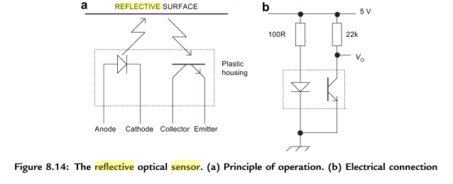
- Length of leads: longer +, shorter -
- Detector connects to sensor signal line
Photocells
- electrically as resistors
- slow response time than photo diode or photo transistor
- suitable for detecting ambient light or as a break-beam sensor
Photo diode or Photo transistor
- more sensitive to small levels of light
- allowing illuminatino source to be a simple LED
- photodetector kind converting light to current or voltage
- photon with sufficient energy striking diode and creating free electron and a hole (inner photoelectric effect)
- absorbtion in depletion region and a wavelength away results in sweeping of carriers (holes towards anode and electrons towards cathode resulting in photocurrent)
- will respond to light particularly longer wavelengths eg red and IR rather visible light.
- I/V characteristic curve with no light on its junction (dark mode) is very similar to a normal signal or rectifying diode.
- reverse current increases as illumination of the junctions increases.
- Disadvantage relatively small current flow
- Advantage fast response time
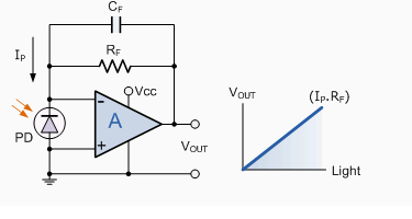
- Photo-current-to-voltage converter circuit
- Vout = Ip * Rf
- Cf to prevent oscillation or gain peaking and to set the output bandwidth (1/2πRC).
- Phototransistor = photodiode with amplification
- collector-base PN-junctoion reverse biased
- NPN Transistor with large base, photons on base produce base current, which causes collector to emitter current to flow
- collector biased +vely wrt emitter => base/collector junction reverse biased => dark current when no light
- advantagemore sensitive and can provide current gain
- transistor to photo diode conversion => photodiode connected between collector and base
Diode
- electronic version of a check valve (pass current in forward direction (forward biased) and block in opposite direction (reverse direction)
- for small currents "signal diode" for large currents "rectifying diode"
- This unidirectional behavior is called rectification
- non linear current-voltage characteristic (non linear resistance and conductance)
- forward biased V is a function of temperature
- 1N4001 rectifying diode for power protection
Semiconductor Diode
![]() crystal of semiconductor
crystal of semiconductor
- impurities added n-type (negative charge carriers) p-type (positive charge carriers)* terminals attached p-n junction
- crystal allows electron flow from n type to p type
- depletion region mobile electrons diffuse into P-doped region leave behind immobile positively charged donor (dopant) on the N side and negatively charged acceptor (dopant) on the P side
- >>region becomes depleted of charge carriers and behaves as an insulator
- recombination proceeds if external voltage polarity opposes the built-in potential silicon diode 0.7V 0.3 V for Germanium and 0.2 V for Schottky
- breakdown causes large increase in current beyond peak inverse voltage PIV, breakdown has small reverse saturation current nA and is temperature dependent at high temp mA, forward but small bias, where only a small forward current is conducted, at cut-in voltage or diode forward voltage drop Vd current–voltage curve is exponential current is acceptable and has very low resistance. http://en.wikipedia.org/wiki/Diode
LED
- when forward biased, electrons combine with holes, emit energy, electro-luminescence and light colour depends upon energy gap,
- a or + long lead is anode and k or - short lead is cathode
LED inner working
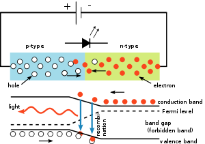
LED I-V diagram
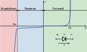
- LED being a diode does not obey Ohms law (not behave linearly) => small increase in voltage results in large increase in current after breakdown voltage (Vforward) => LED may destroy beyond absolute maximum rating IF => Burn instantly if applied 5V (pn-gate destroyed by high current)=> require current limiting resistor (dissipate remaining voltage)(Note: after resistor calculation calculate limiting resistor power dissipation for resistor Watt rating) => choose nearest standard value with a higher resistance
- R depends upon supply V, V drop across LED (Vforward)and desired current (R = VCC - VLED) / ID )
- Omit Limiting Resistor (reduce energy waste, reduce heat dissipation, reduce number of components, reduce PCB cost, reduce component footprint)
- reduce voltage
- use Pulse Width Modulation (PWM)PWM not noticable to human eye and integrates brightness over time (50Hz is used by European Television)
- small LEDs typically draw current upto 10mA - 25mA and high power LEDs require a driver circuit, Vforward(typically 2V for standard red, blue and green LEDs) depends upon LED chemistry, current through LED and temperature.
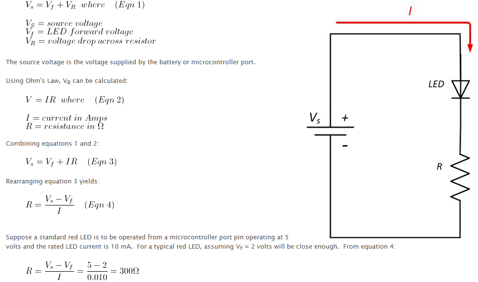 http://www.kpsec.freeuk.com/trancirc.htm
- 300 Ohm is the closest standard value selected from resistor table http://www.eeweb.com/toolbox/resistor-tables http://en.wikipedia.org/wiki/Led
- "Close Enough" Apporximation
- Vf = 2V = Vs - VR(good approx for red and safe for other)
- I = VR / R (if I not close to desired calculate reviser R using Eq 4 and the measured Vf)
OPTEK Technology (POB732WZ Long Distance Reflective Switch)
- opaque housing to reduce the sensor’s ambient light sensitivity.
- emitter and sensor are protected by a clear window, providing a device that can operate in a dusty environment.
- phototransistor can be configured as a Common Collector or Common Emitter device.
- IC(ON) current proportional to the light striking the phototransistor.
- LED => OP240, Phototransistor => OP550
Transistor
- Basic Concept at Bell Labs 1947 (BJT) Reisitor whose value changes, based on the input signal, and the resistance change is transformative (same basic shape as input). http://www.youtube.com/watch?v=CkX8SkTgB0g&feature=related
- BJT small electrical current to control a larger one between collector and emitter, circuit symbol arrow => +ve charge direction, NPN (2N3904)left to right connection (Emitter, Base, Collector => Eat Big Cookie)increase flow with base currentPNP decrease flow with base current
- Common Emitter Mode Emitter is common in the controlling circuit(base current) and (collector current) in controlled circuit => signal at base turns on device attached prior to collector.
- NPN Functional Model base emitter as a diode and collector emitter as a resistance controlled by IB. IC = hFE * IB (where hFE is current gain typically 100). transistor is saturated when full on and RCE = 0 => VCE almost 0 and ICE depends upon supply V and R in collector. circuit.
- Base requires a current limiting resistor RBfor protection
- Selection (a) IC(max) > load current IC (b) hFE> 5 * IC/IC(max) (c) RB = (VC * hFE)/(5*IC) or RB = 0.2*RL*hFE (VC = VS) (d) protection diode if load is motor or relay coil
- two types small signal types and power transistors
- Field Effect Transistor (FET) are controllde by voltage and use almost no input current
http://www.youtube.com/watch?v=-td7YT-Pums&feature=related http://www.kpsec.freeuk.com/trancirc.htm
Relay
- Relay Driver Text http://mbed.org/handbook/Beta
- Low-power circuit to switch a relatively high current on and off
- Control signals electrically isolated from controlling circuit
- Pass suitable pull-in and holding current through its energising coil
- Tutorial [[http://digital-diy.com/general-electronics/99-tip-relays.html]
OP Amp Configeratinos
- voltage source to be sampled is over 5V
- Analogue output between 0 and 24V
- Popular op-amp LM324 (4 amps on board and requires one power supply)
- Non-inverting Amplifier => output greater than input by value of gain.
- gain Vout / Vin = 1 + Rf / R1
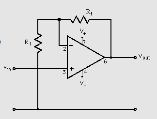
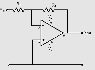
- Inverting Amplifier => sample voltage and reverse polarity while increasing / decreasing output depending upon gain.
- gain Vout / Vin = - Rf / R1
- gain of -1 for equal resistors
- Buffer Amplifier
- Huge input impedance, used to sample circuits with practically no additional load placed on it. http://digital-diy.com/general-electronics/96-tip-op-amp-configerations.html
Pulse Width Modulation
- controls average value of voltage and current fed to a load by switching => works well with digital controls because of on/off nature
- rapidly pulsing digital signal to simulate a varying voltage
- commonly used for driving motors, heaters or lights, Vout = Duty Cycle * Vss
- Terms
- Period: length of time in seconds that the waveform takes to repeat itself
- Frequency: cycles per sec in Hz (how often pulses are generated)
- Duty Cycle is on time expressed in percent of digital 'high' to digital 'low' during PWM period (Duty Cycle = (pulse (that is high time) / cycle (that is,high time + low time ) * 100) => controls voltage (Vavg = Duty Cycle * Vcc) => low duty cycle = low power
- Pulse Width length of activation within a signal
- PWM Resolution: maximum number of pulses that can be packed in to a PWM period (related to frequency)
- LED at 50 Hz duty cycle (used by European Television) time = 1/50 = 0.02 s
- Uses
- To digitally create an analog output voltage level for control functions and power supplies.
- To digitally create analog signals for arbitrary waveforms, sounds, music and speech.
- advantagereduce power loss and heat dissipation
- disadvantage switching current can cause electrical problems
http://www.waitingforfriday.com/index.php/Controlling_LED_brightness_using_PWM
http://www.afrotechmods.com/groovy/PWM_tutorial/PWM_tutorial.htm
http://www.datadog.com/pwm_tutorial.pdf
http://www.electronics-tutorials.ws/waveforms/waveforms.html
calculator: http://www.calctool.org/CALC/phys/optics/pulsed_source
On Oscilloscope http://www3.ntu.edu.sg/home/askklee/scope/Page_6/AppOp6.html
IR Signalling using PWM http://www.hifi-remote.com/infrared/IR-PWM.shtml
http://www.ehow.com/how_8618299_calculate-pulse-width.html
NI http://zone.ni.com/reference/en-XX/help/371361D-01/lvmeasapps/measperiod/
Pulse/Power calculation http://biobionmr.tamu.edu/powerpulsewidthcalculations.htm
Electrical Waveform
visual representation of the variation of a voltage or current over time.
Switched-Mode Power Supply (SMPS)
- power supply incorporating switching regulator to be highly efficient in conversion of electrical power
- pass transistor switches between low-dissipation full on and full-off states and less time in high dissipation transitions
- ideally power supply dissipates no power (in contrast linear power supply regulates output voltage by continually dissipating power in the pass transistor
- voltage regulation achieved by varying on-to-off time
Please log in to post comments.
