Important changes to forums and questions
All forums and questions are now archived. To start a new conversation or read the latest updates go to forums.mbed.com.
8 years, 3 months ago.
CMOS Sensor Addressing Issues?
Hello,
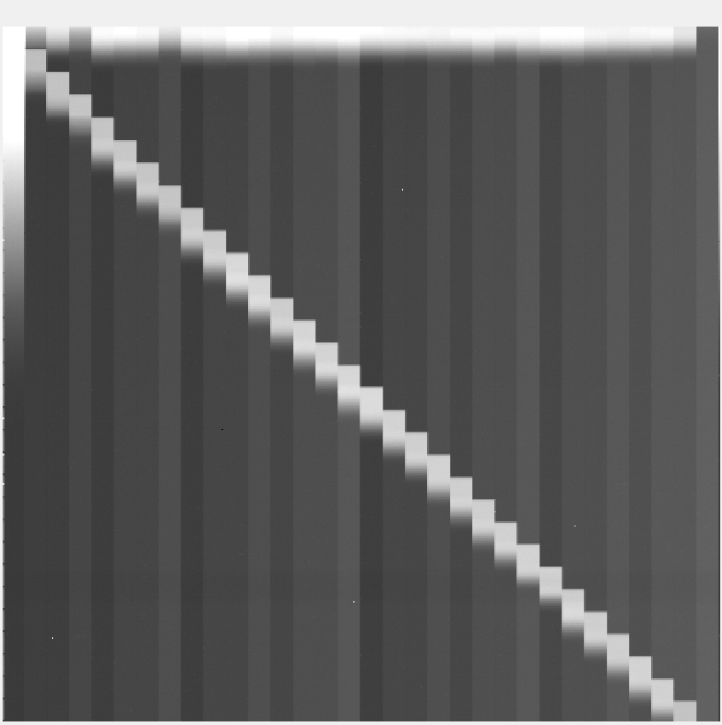
I'm attempting to use my lpc1798 to drive a CMOS image sensor. It seems to be going ok, except for this bizarre staircase feature running down the diagonal of the sensor. It repeats every 16 pixels.

I'm pretty sure it's an addressing issue, since when I run the same frame with the lights on (and the pixels are more or less immediately saturated) the feature disappears.

It's like the mbed is repeating the reset cycle every time it reaches a new "step". Or, whenever Column_Number/Row_Number is some integer multiple of 16. I'm a physics grad student, not a computer or electrical engineer, so this stuff is pretty far out of my wheelhouse. I'd appreciate any help given.
(Note, the large gradient running "North to South" along the columns is from the slow read out of the data. I'm using the USB cable to extract the data, and it's too slow to avoid saturation even under darkness. This will be fixed, so I hope, when I switch to flash memory storage, and don't have to print values on a terminal.)
#include "mbed.h"

Serial pc(USBTX,USBRX);
#define Data_Mask 0x00000FF0
PortOut Data(Port0, Data_Mask);

int Exposures = 100;
float ADCdata;
float realVolt;
int Row_Start = 1;
int Row_Stop = 496;
int Column_Start = 1;
int Column_Stop = 512;
int long Value2 = 0;
int long Value1 = 0;
float dc = 1; //LED duty cycle
int Lframe;

DigitalOut CDS_EN (p12);    //action defined by "ARRAY 1,2....LCC-52 Pin ORDER"
DigitalOut MimGain (p11);    //action defined by "ARRAY 1,2....LCC-52 Pin ORDER"
DigitalOut Snap_RST (p24);    //action defined by "ARRAY 1,2....LCC-52 Pin ORDER"
DigitalOut Row_Ck (p23);    //action defined by "ARRAY 1,2....LCC-52 Pin ORDER"
DigitalOut Clamp (p22);        //action defined by "ARRAY 1,2....LCC-52 Pin ORDER"
DigitalOut TG1_Ck (p19);    //action defined by "ARRAY 1,2....LCC-52 Pin ORDER"
DigitalOut TG2_Ck (p14);    //action defined by "ARRAY 1,2....LCC-52 Pin ORDER"
DigitalOut RST_N_Ck (p15);    //action defined by "ARRAY 1,2....LCC-52 Pin ORDER"
DigitalOut RST_Ck (p16);    //action defined by "ARRAY 1,2....LCC-52 Pin ORDER"
DigitalOut Snap_TG1 (p17);    //action defined by "ARRAY 1,2....LCC-52 Pin ORDER"
DigitalOut Snap_TG2 (p18);    //action defined by "ARRAY 1,2....LCC-52 Pin ORDER"
DigitalOut RedLed(p21);
AnalogIn Ain(p20);


int main()  {
        pc.baud (921600);
        Lframe = Exposures - 1;
        for(int j = 0; j < Exposures; j++) {
            //assumes 496 rows and 512 columns unless changes
            for ( int Row_Number = (Row_Start); Row_Number <= Row_Stop; ++Row_Number) {
                //put correct row address on correct PORT0 pins
                Row_Ck = 0;
                Value2 = Row_Number & 0x00000003;
                Value1 = Row_Number & 0x00000FF0;
                Value1 = Value1 << 2;
                Value1 = Value1 | Value2;
                Data = Value1;        //put data on PORT0 pin
                Row_Ck = 1;       //latch into CMOS imager row address
                RST_Ck = 1;
                RST_Ck = 0;
                float Tint = 0.0001;
                wait(Tint);    //integration time
                TG1_Ck = 1;
                TG2_Ck = 1;
                TG1_Ck = 0;
                TG2_Ck = 0;


                for ( int Column_Number = (Column_Start); Column_Number <= Column_Stop; ++Column_Number) {
                    //put column address on correct PORT0 pin
                    Value2 = Column_Number & 0x00000003;
                    Value1 = Column_Number & 0x00000FF0;
                    Value1 = Value1 << 2;
                    Value1 = Value1 | Value2;
                    Data = Value1;        //put data on PORT0 pin


                    if(j  == Lframe)
                    {
                    ADCdata = Ain;
                    realVolt = ADCdata*(3.3);
                    pc.printf("%.3f \r\n",realVolt);
                    }
                }

            }
        }

}

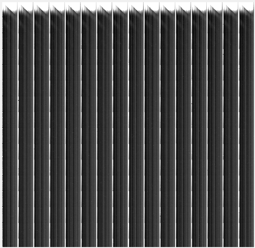
EDIT: The above image is the data provided after the bit shifting suggested below.

EDIT: Another change. It looks like half of the columns look ok, in groups of 16, while the others still have some staircase features that are most prominent on top.
1 Answer
8 years, 3 months ago.
The Issue is with left bit shifting the value to port by <<2 i.e. mulitplying by 4 for both rows and columns for each frame count so you end up with a 4x4=16, you should left shift by 4 mask off and then right shift by 4 to maintain the loop counts you are using. See below
you have...
                Value1 = Row_Number & 0x00000FF0;
                Value1 = Value1 << 2;
should be
                Row_Number=Row_Number << 4;
                Value1 = Row_Number & 0x00000FF0;
                Row_Number = Row_Number >> 4;
and same for columns
Also you don't mention the CMOS sensor you are using but don't you need to 'clock in' the column data?
Thanks a million, I think it's closer, but not quite there yet. I'm sure its another counting error somewhere.
There is no column clock. The row clock is left high, and the columns in that row are read out sequentially.
The code is now...
                Value2 = Row_Number & 0x00000003;
                Row_Number = Row_Number << 4;
                Value1 = Row_Number & 0x00000FF0;
                Row_Number = Row_Number >> 4;
                Value1 = Value1 << 2;
                Value1 = Value1 | Value2;
                Data = Value1;        //put data on PORT0 pin
And the same for the columns
posted by 22 Jan 2016Hi Ben, the thing I can't see is that the Port0 mask is 0x00000FF0 this means only the bits set by 'FF' are actually presented to the port i.e. P0.4 to P0.11 however you shift Value1 bitwise by 2 this should be 4 ? (Since the last 3 digits bit wise is 1111 1111 0000) If you can say which device you are using might get a better handle on the bus/data requirements. Regards
posted by 22 Jan 2016Hey Martin,
First, thanks for the help. The chip is a one-off that was given to my lab to characterize and use for basic science. I'm not sure if it's wise to give out where it came from, so I'm going to avoid that. Suffice it to say, that I personally have very little data on it myself. What I can tell you is that the row/column addressing are tied together on the circuit board and that, for both, the mbed pins used for addressing are as follows, from least significant to most significant:
<0> p9 (P0.0) <1>p10 (P0.1) <2>p30 (P0.4) <3>p29 (P0.5) <4>p8 (P0.6) <5>p7 (P0.7) <6>p6 (P0.8) <7>p5 (P0.9) <8>p28 (P0.10)
Will the 0x00000FF0 mask not let me use the first two bits? I did not write the original driver, but I am the first to attempt to use it with a chip. I recall that the shift of 2 was to accommodate the absence of P0.2 and P0.3 which are both tied to pins being used for other things. Ugh, I feel a bit over my head. Thanks again.
EDIT: I see what you mean about the FF0 mask. I have changed it to 0x00000FF3
posted by 22 Jan 2016Ah OK no worries, now starts to make sense. with the original 0x0000 0FF0 you could only present 8 bits of data at a time but now you've identified that you are using another 2 bits that are 'clocked' in at the same time I can see where you get your range of numbers i.e. 496 rows and 512 columns now. (Since 8 bits are 2^8-1 or 255 and with 10 bits 2^10-1 or 1023 as maximums) OK in your second example remove line 5 with the left shift two, since Value1 should be in the correct position for the bit placement. You are correct with bit Mask for the PortOut class 0x00000FF3 . Kind Regards M
                Value2 = Row_Number & 0x00000003;
                Row_Number = Row_Number << 4;
                Value1 = Row_Number & 0x00000FF0;
                Row_Number = Row_Number >> 4;
                // This will cause an issue Value1 = Value1 << 2;
                Value1 = Value1 | Value2;
                Data = Value1;        //put data on PORT0 pin
Hey Martin,
I tried again, and no luck. I've written a little print out sequence to get a better picture of what's going on, and indeed, the number that's fed doesn't survive into this little machine is changed by the end. I think that the bit shifting is working ok, but the masking itself is doing something weird.
Here's the code:
                    pc.printf("%.8x\t", Column_Number);
                    pc.printf("%.4ld\t", Column_Number);
                    Value2 = Column_Number & 0x00000003;
                    pc.printf("%.8x\t", Value2);
                    pc.printf("%.4ld\t", Value2);
                    Column_Number = Column_Number << 4;
                    Value1 = Column_Number & 0x00000FF0;
                    Column_Number = Column_Number >> 4;
                    pc.printf("%.8x\t", Value1);
                    pc.printf("%.4ld\t", Value1);
                    //Value1 = Value1 << 2;
                    pc.printf("%.8x\t", Value1);
                    pc.printf("%.4ld\t", Value1);
                    Value1 = Value1 | Value2;
                    Data = Value1;        //put data on PORT0 pin
                    pc.printf("%.8x\t", Value1);
                    pc.printf("%.4ld\r\n", Value1);
And, here's some of what's been printing out. First with the shifting you suggested.
0000008a        0138    00000002        0002    000008a0        2208    000008a0        2208    000008a2        2210
0000008b        0139    00000003        0003    000008b0        2224    000008b0        2224    000008b3        2227
0000008c        0140    00000000        0000    000008c0        2240    000008c0        2240    000008c0        2240
And now with the original shifting.
0000008a        0138    00000002        0002    00000080        0128    00000200        0512    00000202        0514
0000008b        0139    00000003        0003    00000080        0128    00000200        0512    00000203        0515
0000008c        0140    00000000        0000    00000080        0128    00000200        0512    00000200        0512
Sorry for the weird editing, I tried to make the print out easier to read.
Neither of these give the correct binary number post processing (everything from the third bit shifted 2 to the left)
As always, thanks so much for the help.
Ben
posted by 25 Jan 2016ok final stab at this just tried a small script and this 'should' work. The orignal problem was you masked off lower 4 bits and then left shifted by 2 and of course you then lost 2 bits on the way. I was confused by the masking off and lower 4 bits. The order of code should be as follows that is left shift by TWO (That was right) THEN mask off lower four bits this means you will have "8bits data + 2 Zero bits + 2bits data"... i.e. xxxx xxxx 00 xx where x's are your data
                Value2 = Row_Number & 0x00000003;
                Row_Number = Row_Number << 2;
                Value1 = Row_Number & 0x00000FF0;
                Row_Number = Row_Number >> 2;
                Value1 = Value1 | Value2;
                Data = Value1;        //put data on PORT0 pin
or more condensed
                Value2 = Row_Number & 0x00000003;
                Value1 = (Row_Number << 2)& 0x00000FF0;
                Data = Value1 | Value2;   //put data on PORT0 pin
isn't there a difference between ++variable and variable++ First instance you start from variable +1 Second instance you start from Variable Check lines 39 and 58 Justed checked ignore above...
posted by Martin Simpson 22 Jan 2016