ARM Cortex-M3 DesignStart
ARM® Cortex-M3 DesignStart™ Eval allows design teams to design, simulate, and prototype the digital elements of their custom SoC. Through Cortex-M3 DesignStart developers can get free and instant access the Cortex-M3 processor and CoreLink SSE-050 subsystem for design, simulation and then prototyping on the ARM MPS2+ FPGA Prototyping System+. Cortex-M3 DesignStart has out-of-the-box support for mbed™OS and mbed Cloud, enabling developers to quickly and easily integrate their design with their cloud IoT application.

Subsystem Information
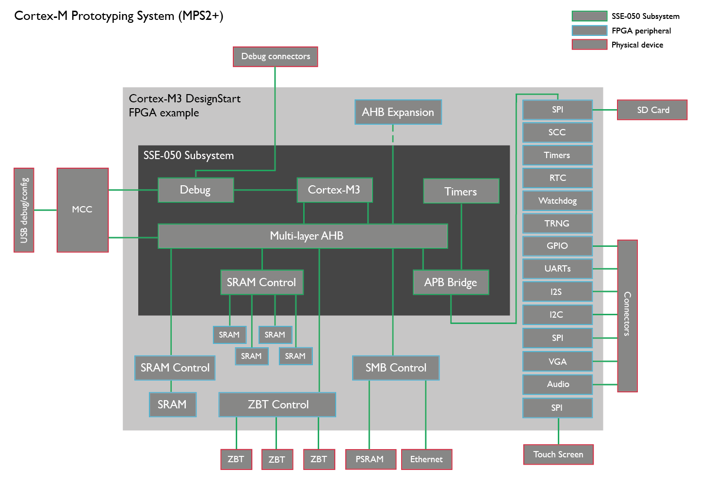
The Cortex-M3 DesignStart Eval example system includes all of the components and peripherals which are required to implement a complete SoC system on the MPS2+ FPGA platform, including the Cortex-M3 processor, a subsystem, a standard set of peripherals designed to support software development for an IoT endpoint, combined with full support of mbed™OS and mbed Cloud. The DesignStart Eval package provides an RTL simulation environment, and the ability to extend the design to produce a customised FPGA image. In addition to the standard peripherals provided by the MPS2+ FPGA Prototyping system, the Cortex-M3 DesignStart Eval example system provides the following peripherals:
- Two timers dedicated to use by the mbed OS
- Timers, UART, Watchdog, RTC and True Random Number Generator for application use
- SPI interface for micro SD-card
The Cortex-M3 processor and subsystem are also available for full licensing through Cortex-M3 DesignStart Pro – providing a free of charge license to Cortex-M3 and the CoreLink SSE-050 subsystem for full SoC development, manufacturing and commercialization.
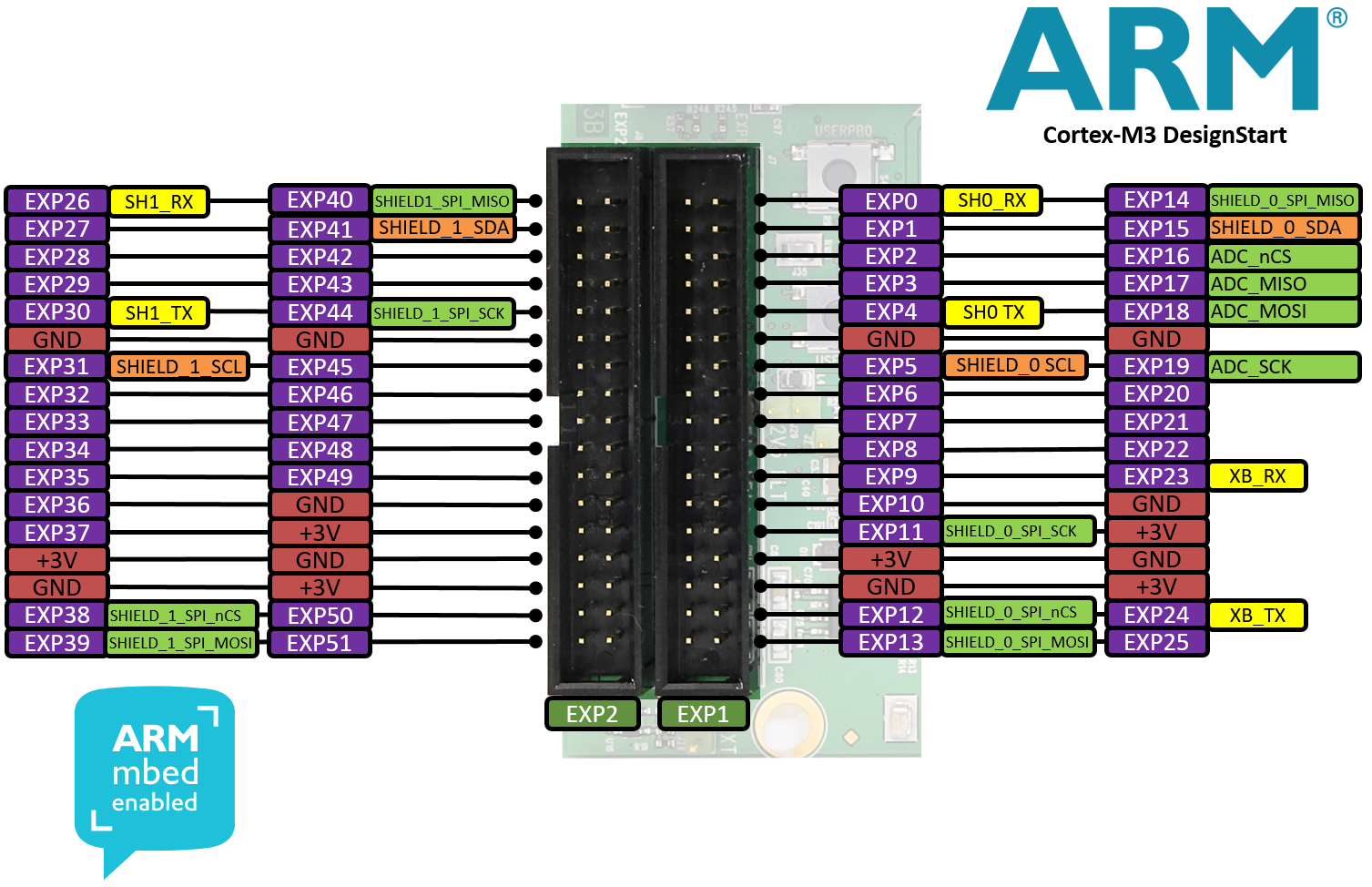
Pinout


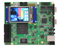
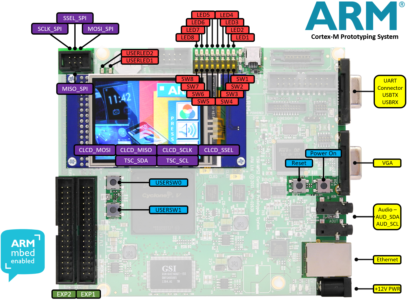
Cortex-M3 DesignStart Eval implementation in FPGA

Features
- Form factor: 140x120cm
- SRAM: 8MB single cycle SRAM, 16MB PSRAM
- Two additional 4MB regions - 1 RAM and 1 FLASH
- Video: QSVGA touch screen panel, 4bit RGB VGA connector
- Audio: Audio Codec
- Debug: ◦ARM JTAG20 connector
- ARM parallel trace connector (MICTOR38)
- 20 pin Cortex debug connector
- 10 pin Cortex debug connector
- ILA connector for FPGA debug
- Expansion
- GPIO
- SPI
- MPS2+ Datasheet
- MPS2+ Technical Reference Manual
- MPS2+ Product web page
- Register for Cortex-M3 DesignStart Eval to download the FPGA image
Getting Started
The CMSIS-DAP support for this platform is provided by the baseboard bios. You need mbb_v221 (included with the DesignStart bundle) or later. The latest firmware version is mbb_v266, and this is available on the DesignStart community.
CMSIS-DAP on the MPS2+ does not support a UART over the same USB connection, you must use the DB-9 connector and supplied cable.
When you download a compiled image to the FPGA, be sure to use an 8:3 format file name, and reference this file name in V2M_MPS2:\MB\HBI0263C\AN511\images.txt (if the bin file is in the SOFTWARE directory), or place a single .bin file in the root directory of the V2M_MPS2: drive (which will override the image specified in the current images.txt file).
For more details, see the FPGA user guide and the RTL user guide
Note Timer0 and Timer1 (at 0x4000_0000 and 0x4000_1000) are reserved for use as the low-power timer by mbed-os, and should be implemented in an always-on domain if power domains are added to your platform.
For more information about testing the uSD card over SPI, see this thread on the Arm Community.
The MPS2+ FPGA board can also be used with various encrypted implementations of the Cortex-M processor range, but these provide a simpler CMSDK based memory map, and must be used with the ARM-MPS2 board configuration.
You need to log in to post a discussion
